Intel BX80571E5300 Data Sheet - Page 18
DC Voltage and Current Specification - e5300
 |
UPC - 735858204996
View all Intel BX80571E5300 manuals
Add to My Manuals
Save this manual to your list of manuals |
Page 18 highlights
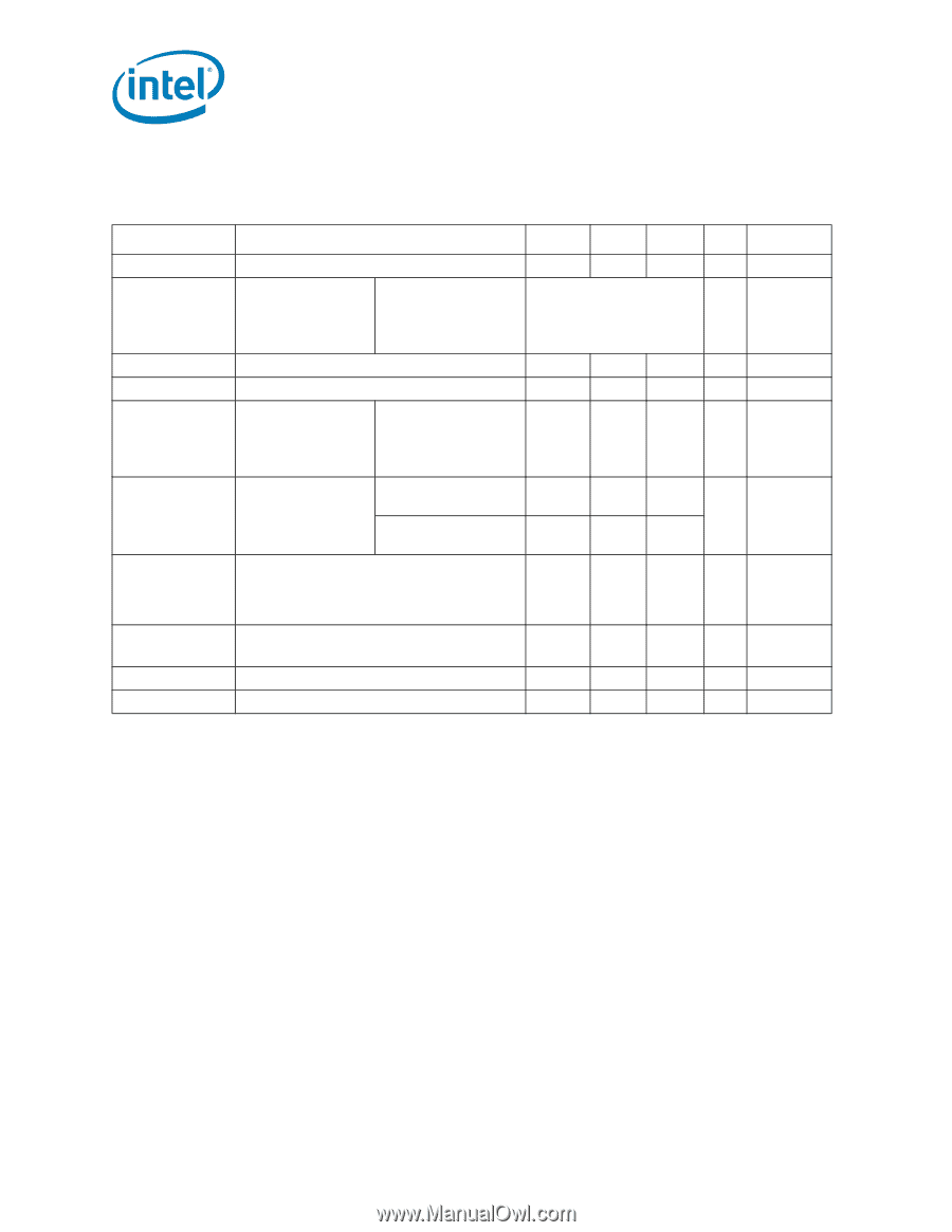
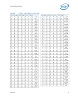
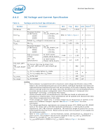
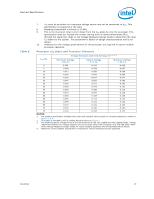
Electrical Specifications 2.6.2 DC Voltage and Current Specification Table 4. Voltage and Current Specifications Symbol Parameter Min Typ Max Unit Notes2, 10 VID Range VID 0.8500 - 1.3625 V 1 Core VCC Processor Number (2 MB Cache): E5200 E5300 VCC for 775_VR_CONFIG_06: 2.50 GHz 2.66 GHz Refer to Table 5, Figure 1 V 3, 4, 5 VCC_BOOT VCCPLL ICC Default VCC voltage for initial power up PLL VCC Processor Number (2 MB Cache): VCC for 775_VR_CONFIG_06: E5200 2.50 GHz E5300 2.66 GHz - - 5% - 1.10 1.50 - + 5% - 75 75 V V A6 FSB termination voltage on Intel 3 series Chipset family boards 1.045 1.1 1.155 VTT (DC + AC specifications) on Intel 4 series Chipset family boards 1.14 V 7, 8 1.2 1.26 VTT_OUT_LEFT and VTT_OUT_RIGHT ICC ITT ICC_VCCPLL ICC_GTLREF DC Current that may be drawn from VTT_OUT_LEFT and VTT_OUT_RIGHT per land ICC for VTT supply before VCC stable ICC for VTT supply after VCC stable ICC for PLL land ICC for GTLREF - - 580 mA 4.5 - - A9 4.6 - - 130 mA - - 200 µA NOTES: 1. Each processor is programmed with a maximum valid voltage identification value (VID), which is set at manufacturing and can not be altered. Individual maximum VID values are calibrated during manufacturing such that two processors at the same frequency may have different settings within the VID range. Note that this differs from the VID employed by the processor during a power management event (Thermal Monitor 2, Enhanced Intel SpeedStep® technology, or Extended HALT State). 2. Unless otherwise noted, all specifications in this table are based on estimates and simulations or empirical data. These specifications will be updated with characterized data from silicon measurements at a later date. 3. These voltages are targets only. A variable voltage source should exist on systems in the event that a different voltage is required. See Section 2.3 and Table 2 for more information. 4. The voltage specification requirements are measured across VCC_SENSE and VSS_SENSE lands at the socket with a 100 MHz bandwidth oscilloscope, 1.5 pF maximum probe capacitance, and 1 MΩ minimum impedance. The maximum length of ground wire on the probe should be less than 5 mm. Ensure external noise from the system is not coupled into the oscilloscope probe. 5. Refer to Table 5 and Figure 1, for the minimum, typical, and maximum VCC allowed for a given current. The processor should not be subjected to any VCC and ICC combination wherein VCC exceeds VCC_MAX for a given current. 6. ICC_MAX specification is based on VCC_MAX loadline. Refer to Figure 1 for details. 18 Datasheet
-
 1
1 -
2
-
3
-
4
-
5
-
6
-
7
-
8
-
9
-
10
-
11
-
12
-
 13
13 -
 14
14 -
 15
15 -
 16
16 -
 17
17 -
 18
18 -
 19
19 -
 20
20 -
 21
21 -
 22
22 -
 23
23 -
24
-
25
-
26
-
27
-
28
-
29
-
30
-
31
-
32
-
33
-
34
-
35
-
36
-
37
-
38
-
39
-
40
-
41
-
42
-
43
-
44
-
45
-
46
-
47
-
48
-
49
-
50
-
51
-
52
-
53
-
54
-
55
-
56
-
57
-
58
-
59
-
60
-
61
-
62
-
63
-
64
-
65
-
66
-
67
-
68
-
69
-
70
-
71
-
72
-
73
-
74
-
75
-
76
-
77
-
78
-
79
-
80
-
81
-
82
-
83
-
84
-
85
-
86
-
87
-
88
-
89
-
90
-
91
-
92
-
93
-
94
-
95
-
96
-
97
-
98
-
99
-
100
 |
 |