Intel BX80571E5300 Data Sheet - Page 69
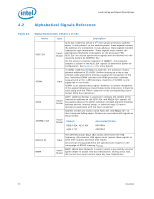
Table 24., Signal Description, Sheet 6 of 10 - atom
 |
UPC - 735858204996
View all Intel BX80571E5300 manuals
Add to My Manuals
Save this manual to your list of manuals |
Page 69 highlights
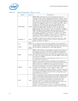
Land Listing and Signal Descriptions Table 24. Signal Description (Sheet 6 of 10) Name Type Description ITP_CLK[1:0] LINT[1:0] LOCK# MSID[1:0] PECI PROCHOT# PSI# Input ITP_CLK[1:0] are copies of BCLK that are used only in processor systems where no debug port is implemented on the system board. ITP_CLK[1:0] are used as BCLK[1:0] references for a debug port implemented on an interposer. If a debug port is implemented in the system, ITP_CLK[1:0] are no connects in the system. These are not processor signals. Input LINT[1:0] (Local APIC Interrupt) must connect the appropriate pins/lands of all APIC Bus agents. When the APIC is disabled, the LINT0 signal becomes INTR, a maskable interrupt request signal, and LINT1 becomes NMI, a nonmaskable interrupt. INTR and NMI are backward compatible with the signals of those names on the Pentium processor. Both signals are asynchronous. Both of these signals must be software configured via BIOS programming of the APIC register space to be used either as NMI/ INTR or LINT[1:0]. Because the APIC is enabled by default after Reset, operation of these signals as LINT[1:0] is the default configuration. Input/ Output LOCK# indicates to the system that a transaction must occur atomically. This signal must connect the appropriate pins/lands of all processor FSB agents. For a locked sequence of transactions, LOCK# is asserted from the beginning of the first transaction to the end of the last transaction. When the priority agent asserts BPRI# to arbitrate for ownership of the processor FSB, it will wait until it observes LOCK# de-asserted. This enables symmetric agents to retain ownership of the processor FSB throughout the bus locked operation and ensure the atomicity of lock. Output On the processor these signals are connected on the package to Vss. As an alternative to MSID, Intel has implemented the Power Segment Identifier (PSID) to report the maximum Thermal Design Power of the processor. Refer to Section 2.5 for additional information regarding PSID. Input/ PECI is a proprietary one-wire bus interface. See Chapter 5.3 for Output details. Input/ Output As an output, PROCHOT# (Processor Hot) will go active when the processor temperature monitoring sensor detects that the processor has reached its maximum safe operating temperature. This indicates that the processor Thermal Control Circuit (TCC) has been activated, if enabled. As an input, assertion of PROCHOT# by the system will activate the TCC, if enabled. The TCC will remain active until the system de-asserts PROCHOT#. See Section 5.2.4 for more details. Output Processor Power Status Indicator Signal. This signal may be asserted when the processor is in the Deeper Sleep State. PSI# can be used to improve load efficiency of the voltage regulator, resulting in platfrom power savings. Datasheet 69
-
 1
1 -
2
-
3
-
4
-
5
-
6
-
7
-
8
-
9
-
10
-
11
-
12
-
13
-
14
-
15
-
16
-
17
-
18
-
19
-
20
-
21
-
22
-
23
-
24
-
25
-
26
-
27
-
28
-
29
-
30
-
31
-
32
-
33
-
34
-
35
-
36
-
37
-
38
-
39
-
40
-
41
-
42
-
43
-
44
-
45
-
46
-
47
-
48
-
49
-
50
-
51
-
52
-
53
-
54
-
55
-
56
-
57
-
58
-
59
-
60
-
61
-
62
-
63
-
 64
64 -
 65
65 -
 66
66 -
 67
67 -
 68
68 -
 69
69 -
 70
70 -
 71
71 -
 72
72 -
 73
73 -
 74
74 -
75
-
76
-
77
-
78
-
79
-
80
-
81
-
82
-
83
-
84
-
85
-
86
-
87
-
88
-
89
-
90
-
91
-
92
-
93
-
94
-
95
-
96
-
97
-
98
-
99
-
100
 |
 |