Intel BX80571E5300 Data Sheet - Page 58
Datasheet, Power/Other, PWRGOOD, Input, IGNNE, Asynch CMOS, RESERVED, DPSLP, Source Synch, Input/
 |
UPC - 735858204996
View all Intel BX80571E5300 manuals
Add to My Manuals
Save this manual to your list of manuals |
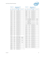
Page 58 highlights
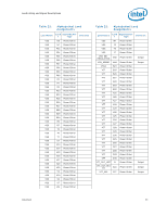
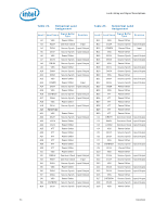
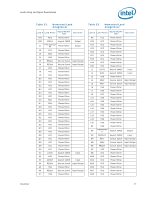
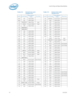
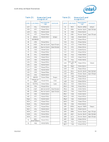
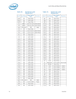
Land Listing and Signal Descriptions Table 23. Numerical Land Assignment Land # Land Name Signal Buffer Type Direction M29 M30 N1 N2 N3 VCC VCC PWRGOOD IGNNE# VSS Power/Other Power/Other Power/Other Asynch CMOS Power/Other Input Input N4 RESERVED N5 RESERVED N6 VSS Power/Other N7 VSS Power/Other N8 VCC Power/Other N23 VCC Power/Other N24 VCC Power/Other N25 VCC Power/Other N26 VCC Power/Other N27 VCC Power/Other N28 VCC Power/Other N29 VCC Power/Other N30 VCC Power/Other P1 DPSLP# Asynch CMOS Input P2 SMI# Asynch CMOS Input P3 INIT# Asynch CMOS Input P4 VSS Power/Other P5 RESERVED P6 A04# Source Synch Input/Output P7 VSS Power/Other P8 VCC Power/Other P23 VSS Power/Other P24 VSS Power/Other P25 VSS Power/Other P26 VSS Power/Other P27 VSS Power/Other P28 VSS Power/Other P29 VSS Power/Other P30 VSS Power/Other R1 COMP3 Power/Other Input R2 VSS Power/Other R3 FERR#/PBE# Asynch CMOS Output R4 A08# Source Synch Input/Output R5 VSS Power/Other Table 23. Numerical Land Assignment Land # Land Name Signal Buffer Type Direction R6 ADSTB0# Source Synch Input/Output R7 VSS Power/Other R8 VCC Power/Other R23 VSS Power/Other R24 VSS Power/Other R25 R26 R27 R28 R29 R30 T1 T2 T3 T4 T5 T6 T7 T8 T23 T24 T25 T26 T27 T28 T29 T30 U1 U2 U3 U4 U5 U6 U7 U8 U23 U24 U25 U26 VSS VSS VSS VSS VSS VSS COMP1 DPRSTP# VSS A11# A09# VSS VSS VCC VCC VCC VCC VCC VCC VCC VCC VCC FC28 FC29 FC30 A13# A12# A10# VSS VCC VCC VCC VCC VCC Power/Other Power/Other Power/Other Power/Other Power/Other Power/Other Power/Other Input Asynch CMOS Input Power/Other Source Synch Input/Output Source Synch Input/Output Power/Other Power/Other Power/Other Power/Other Power/Other Power/Other Power/Other Power/Other Power/Other Power/Other Power/Other Power/Other Power/Other Power/Other Source Synch Input/Output Source Synch Input/Output Source Synch Input/Output Power/Other Power/Other Power/Other Power/Other Power/Other Power/Other 58 Datasheet
-
 1
1 -
2
-
3
-
4
-
5
-
6
-
7
-
8
-
9
-
10
-
11
-
12
-
13
-
14
-
15
-
16
-
17
-
18
-
19
-
20
-
21
-
22
-
23
-
24
-
25
-
26
-
27
-
28
-
29
-
30
-
31
-
32
-
33
-
34
-
35
-
36
-
37
-
38
-
39
-
40
-
41
-
42
-
43
-
44
-
45
-
46
-
47
-
48
-
49
-
50
-
51
-
52
-
 53
53 -
 54
54 -
 55
55 -
 56
56 -
 57
57 -
 58
58 -
 59
59 -
 60
60 -
 61
61 -
 62
62 -
 63
63 -
64
-
65
-
66
-
67
-
68
-
69
-
70
-
71
-
72
-
73
-
74
-
75
-
76
-
77
-
78
-
79
-
80
-
81
-
82
-
83
-
84
-
85
-
86
-
87
-
88
-
89
-
90
-
91
-
92
-
93
-
94
-
95
-
96
-
97
-
98
-
99
-
100
 |
 |
