Intel BX80571E5300 Data Sheet - Page 22
FSB Signal Groups
 |
UPC - 735858204996
View all Intel BX80571E5300 manuals
Add to My Manuals
Save this manual to your list of manuals |
Page 22 highlights
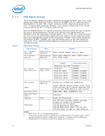
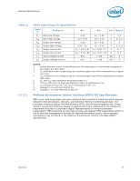
Electrical Specifications 2.7.1 Table 7. FSB Signal Groups The front side bus signals have been combined into groups by buffer type. GTL+ input signals have differential input buffers, which use GTLREF[1:0] as a reference level. In this document, the term "GTL+ Input" refers to the GTL+ input group as well as the GTL+ I/O group when receiving. Similarly, "GTL+ Output" refers to the GTL+ output group as well as the GTL+ I/O group when driving. With the implementation of a source synchronous data bus comes the need to specify two sets of timing parameters. One set is for common clock signals which are dependent upon the rising edge of BCLK0 (ADS#, HIT#, HITM#, etc.) and the second set is for the source synchronous signals which are relative to their respective strobe lines (data and address) as well as the rising edge of BCLK0. Asychronous signals are still present (A20M#, IGNNE#, etc.) and can become active at any time during the clock cycle. Table 7 identifies which signals are common clock, source synchronous, and asynchronous. FSB Signal Groups Signal Group Type Signals1 GTL+ Common Clock Input GTL+ Common Clock I/O Synchronous to BCLK[1:0] Synchronous to BCLK[1:0] BPRI#, DEFER#, RESET#, RS[2:0]#, TRDY# ADS#, BNR#, BPM[5:0]#, BR0#3, DBSY#, DRDY#, HIT#, HITM#, LOCK# GTL+ Source Synchronous I/O Synchronous to assoc. strobe Signals REQ[4:0]#, A[16:3]#3 A[35:17]#3 D[15:0]#, DBI0# D[31:16]#, DBI1# D[47:32]#, DBI2# D[63:48]#, DBI3# Associated Strobe ADSTB0# ADSTB1# DSTBP0#, DSTBN0# DSTBP1#, DSTBN1# DSTBP2#, DSTBN2# DSTBP3#, DSTBN3# GTL+ Strobes CMOS Open Drain Output Open Drain Input/ Output FSB Clock Power/Other Synchronous to BCLK[1:0] Clock ADSTB[1:0]#, DSTBP[3:0]#, DSTBN[3:0]# A20M#, DPRSTP#. DPSLP#, IGNNE#, INIT#, LINT0/ INTR, LINT1/NMI, SMI#3, STPCLK#, PWRGOOD, SLP#, TCK, TDI, TMS, TRST#, BSEL[2:0], VID[7:0], PSI# FERR#/PBE#, IERR#, THERMTRIP#, TDO PROCHOT#4 BCLK[1:0], ITP_CLK[1:0]2 VCC, VTT, VCCA, VCCIOPLL, VCCPLL, VSS, VSSA, GTLREF[1:0], COMP[8,3:0], RESERVED, TESTHI[12,10:0], VCC_SENSE, VCC_MB_REGULATION, VSS_SENSE, VSS_MB_REGULATION, DBR#2, VTT_OUT_LEFT, VTT_OUT_RIGHT, VTT_SEL, FCx, PECI, MSID[1:0] NOTES: 1. Refer to Section 4.2 for signal descriptions. 2. In processor systems where no debug port is implemented on the system board, these signals are used to support a debug port interposer. In systems with the debug port implemented on the system board, these signals are no connects. 22 Datasheet
-
 1
1 -
2
-
3
-
4
-
5
-
6
-
7
-
8
-
9
-
10
-
11
-
12
-
13
-
14
-
15
-
16
-
 17
17 -
 18
18 -
 19
19 -
 20
20 -
 21
21 -
 22
22 -
 23
23 -
 24
24 -
 25
25 -
 26
26 -
 27
27 -
28
-
29
-
30
-
31
-
32
-
33
-
34
-
35
-
36
-
37
-
38
-
39
-
40
-
41
-
42
-
43
-
44
-
45
-
46
-
47
-
48
-
49
-
50
-
51
-
52
-
53
-
54
-
55
-
56
-
57
-
58
-
59
-
60
-
61
-
62
-
63
-
64
-
65
-
66
-
67
-
68
-
69
-
70
-
71
-
72
-
73
-
74
-
75
-
76
-
77
-
78
-
79
-
80
-
81
-
82
-
83
-
84
-
85
-
86
-
87
-
88
-
89
-
90
-
91
-
92
-
93
-
94
-
95
-
96
-
97
-
98
-
99
-
100
 |
 |
