Intel BX80571E5300 Data Sheet - Page 67
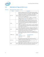
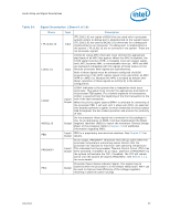
Table 24., Signal Description, Sheet 4 of 10
 |
UPC - 735858204996
View all Intel BX80571E5300 manuals
Add to My Manuals
Save this manual to your list of manuals |
Page 67 highlights
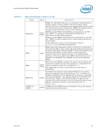
Land Listing and Signal Descriptions Table 24. Signal Description (Sheet 4 of 10) Name Type Description DEFER# DPRSTP# DPSLP# DRDY# Input DEFER# is asserted by an agent to indicate that a transaction cannot be ensured in-order completion. Assertion of DEFER# is normally the responsibility of the addressed memory or input/ output agent. This signal must connect the appropriate pins/lands of all processor FSB agents. Input DPRSTP#, when asserted on the platform, causes the processor to transition from the Deep Sleep State to the Deeper Sleep state. To return to the Deep Sleep State, DPRSTP# must be deasserted. Use of the DPRSTP# pin, and corresponding low power state, requires chipset support and may not be available on all platforms. NOTE: Some processors may not have the Deeper Sleep State enabled, refer to the Specification Update for specific sku and stepping guidance. Input DPSLP#, when asserted on the platform, causes the processor to transition from the Sleep State to the Deep Sleep state. To return to the Sleep State, DPSLP# must be deasserted. Use of the DPSLP# pin, and corresponding low power state, requires chipset support and may not be available on all platforms. NOTE: Some processors may not have the Deep Sleep State enabled, refer to the Specification Update for specific proceswor and stepping guidance. Input/ Output DRDY# (Data Ready) is asserted by the data driver on each data transfer, indicating valid data on the data bus. In a multi-common clock data transfer, DRDY# may be de-asserted to insert idle clocks. This signal must connect the appropriate pins/lands of all processor FSB agents. DSTBN[3:0]# are the data strobes used to latch in D[63:0]#. DSTBN[3:0]# Input/ Output Signals D[15:0]#, DBI0# D[31:16]#, DBI1# D[47:32]#, DBI2# D[63:48]#, DBI3# Associated Strobe DSTBN0# DSTBN1# DSTBN2# DSTBN3# DSTBP[3:0]# are the data strobes used to latch in D[63:0]#. DSTBP[3:0]# Input/ Output Signals D[15:0]#, DBI0# D[31:16]#, DBI1# D[47:32]#, DBI2# D[63:48]#, DBI3# Associated Strobe DSTBP0# DSTBP1# DSTBP2# DSTBP3# FC0/BOOTSELECT FCx Other Other FC0/BOOTSELECT is not used by the processor. When this land is tied to Vss previous processors based on the Intel NetBurst® microarchitecture should be disabled and prevented from booting. FC signals are signals that are available for compatibility with other processors. Datasheet 67
-
 1
1 -
2
-
3
-
4
-
5
-
6
-
7
-
8
-
9
-
10
-
11
-
12
-
13
-
14
-
15
-
16
-
17
-
18
-
19
-
20
-
21
-
22
-
23
-
24
-
25
-
26
-
27
-
28
-
29
-
30
-
31
-
32
-
33
-
34
-
35
-
36
-
37
-
38
-
39
-
40
-
41
-
42
-
43
-
44
-
45
-
46
-
47
-
48
-
49
-
50
-
51
-
52
-
53
-
54
-
55
-
56
-
57
-
58
-
59
-
60
-
61
-
 62
62 -
 63
63 -
 64
64 -
 65
65 -
 66
66 -
 67
67 -
 68
68 -
 69
69 -
 70
70 -
 71
71 -
 72
72 -
73
-
74
-
75
-
76
-
77
-
78
-
79
-
80
-
81
-
82
-
83
-
84
-
85
-
86
-
87
-
88
-
89
-
90
-
91
-
92
-
93
-
94
-
95
-
96
-
97
-
98
-
99
-
100
 |
 |
