Intel BX80571E5300 Data Sheet - Page 56
Power/Other
 |
UPC - 735858204996
View all Intel BX80571E5300 manuals
Add to My Manuals
Save this manual to your list of manuals |
Page 56 highlights
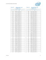
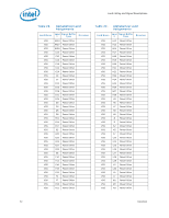
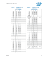
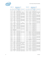
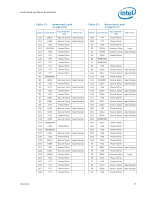
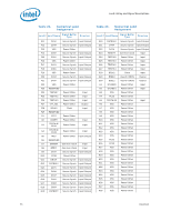
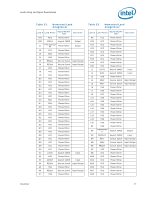
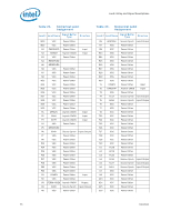
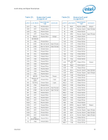
Land Listing and Signal Descriptions Table 23. Numerical Land Assignment Land # Land Name Signal Buffer Type Direction F11 D23# Source Synch Input/Output F12 D24# Source Synch Input/Output F13 VSS Power/Other F14 D28# Source Synch Input/Output F15 D30# Source Synch Input/Output F16 F17 F18 F19 F20 F21 F22 F23 F24 F25 F26 F27 F28 F29 G1 G2 G3 G4 G5 G6 G7 G8 G9 G10 G11 G12 G13 G14 G15 G16 G17 G18 G19 VSS Power/Other D37# Source Synch Input/Output D38# Source Synch Input/Output VSS Power/Other D41# Source Synch Input/Output D43# Source Synch Input/Output VSS Power/Other RESERVED TESTHI7 Power/Other Input TESTHI2 Power/Other Input TESTHI0 Power/Other Input VTT_SEL Power/Other Output BCLK0 Clock Input RESERVED FC27 Power/Other COMP2 Power/Other Input TESTHI8/ FC42 Power/Other Input TESTHI9/ FC43 Power/Other Input PECI Power/Other Input/Output RESERVED DEFER# Common Clock Input BPRI# Common Clock Input D16# Source Synch Input/Output FC38 Power/Other DBI1# Source Synch Input/Output DSTBN1# Source Synch Input/Output D27# Source Synch Input/Output D29# Source Synch Input/Output D31# Source Synch Input/Output D32# Source Synch Input/Output D36# Source Synch Input/Output D35# Source Synch Input/Output DSTBP2# Source Synch Input/Output Table 23. Numerical Land Assignment Land # Land Name Signal Buffer Type Direction G20 G21 G22 G23 G24 DSTBN2# D44# D47# RESET# TESTHI6 Source Synch Input/Output Source Synch Input/Output Source Synch Input/Output Common Clock Input Power/Other Input G25 G26 G27 G28 G29 G30 H1 H2 H3 H4 H5 H6 H7 H8 H9 H10 H11 H12 H13 H14 H15 H16 H17 H18 H19 H20 H21 H22 H23 H24 H25 H26 H27 H28 TESTHI3 TESTHI5 TESTHI4 BCLK1 BSEL0 BSEL2 GTLREF0 GTLREF1 VSS FC35 TESTHI10 VSS VSS VSS VSS VSS VSS VSS VSS VSS FC32 FC33 VSS VSS VSS VSS VSS VSS VSS VSS VSS VSS VSS VSS Power/Other Power/Other Power/Other Clock Asynch CMOS Asynch CMOS Power/Other Power/Other Power/Other Power/Other Power/Other Power/Other Power/Other Power/Other Power/Other Power/Other Power/Other Power/Other Power/Other Power/Other Power/Other Power/Other Power/Other Power/Other Power/Other Power/Other Power/Other Power/Other Power/Other Power/Other Power/Other Power/Other Power/Other Power/Other Input Input Input Input Output Output Input Input Input 56 Datasheet
-
 1
1 -
2
-
3
-
4
-
5
-
6
-
7
-
8
-
9
-
10
-
11
-
12
-
13
-
14
-
15
-
16
-
17
-
18
-
19
-
20
-
21
-
22
-
23
-
24
-
25
-
26
-
27
-
28
-
29
-
30
-
31
-
32
-
33
-
34
-
35
-
36
-
37
-
38
-
39
-
40
-
41
-
42
-
43
-
44
-
45
-
46
-
47
-
48
-
49
-
50
-
 51
51 -
 52
52 -
 53
53 -
 54
54 -
 55
55 -
 56
56 -
 57
57 -
 58
58 -
 59
59 -
 60
60 -
 61
61 -
62
-
63
-
64
-
65
-
66
-
67
-
68
-
69
-
70
-
71
-
72
-
73
-
74
-
75
-
76
-
77
-
78
-
79
-
80
-
81
-
82
-
83
-
84
-
85
-
86
-
87
-
88
-
89
-
90
-
91
-
92
-
93
-
94
-
95
-
96
-
97
-
98
-
99
-
100
 |
 |
