Toshiba DVR610 Service Manual - Page 79
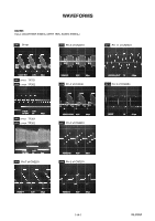
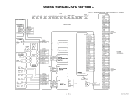
Ic1571 Vfd Driver
 |
UPC - 022265001370
View all Toshiba DVR610 manuals
Add to My Manuals
Save this manual to your list of manuals |
Page 79 highlights
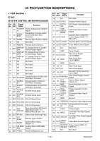
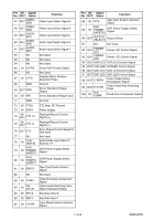
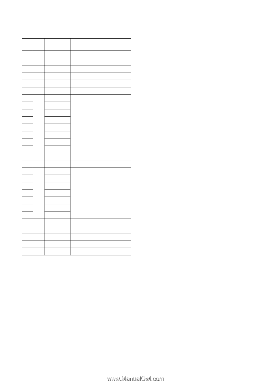
< DVD Section > IC1571 (VFD DRIVER) Pin IN/ Signal No. OUT Name 1 IN CLK 2 IN STB 3 - NU 4 - NU 5 - VSS 6 - VDD 7 P9 8 P8 9 P1 10 P2 OUT 11 P3 12 P4 13 P5 14 P6 15 - VEE 16 OUT P7 17 7G 18 6G 19 5G 20 OUT 4G 21 3G 22 2G 23 1G 24 - VDD 25 - VSS 26 IN OSC 27 - NU 28 IN DIN Function Clock Input Serial Interface Strobe Not Used Not Used Ground Power Supply Segment Output Pull Down Level Segment Output Grid Output Power Supply Ground Oscillator Input Not Used Serial Data Input 1-16-3 E9KGAPIN
-
 1
1 -
2
-
3
-
4
-
5
-
6
-
7
-
8
-
9
-
10
-
11
-
12
-
13
-
14
-
15
-
16
-
17
-
18
-
19
-
20
-
21
-
22
-
23
-
24
-
25
-
26
-
27
-
28
-
29
-
30
-
31
-
32
-
33
-
34
-
35
-
36
-
37
-
38
-
39
-
40
-
41
-
42
-
43
-
44
-
45
-
46
-
47
-
48
-
49
-
50
-
51
-
52
-
53
-
54
-
55
-
56
-
57
-
58
-
59
-
60
-
61
-
62
-
63
-
64
-
65
-
66
-
67
-
68
-
69
-
70
-
71
-
72
-
73
-
 74
74 -
 75
75 -
 76
76 -
 77
77 -
 78
78 -
 79
79 -
 80
80 -
 81
81 -
 82
82 -
 83
83 -
 84
84 -
85
-
86
-
87
 |
 |
1-16-3
E9KGAPIN
< DVD Section >
IC1571 (VFD DRIVER)
Pin
No.
IN/
OUT
Signal
Name
Function
1
IN CLK
Clock Input
2
IN STB
Serial Interface Strobe
3
-
NU
Not Used
4
-
NU
Not Used
5
-
VSS
Ground
6
-
VDD
Power Supply
7
OUT
P9
Segment Output
8
P8
9
P1
10
P2
11
P3
12
P4
13
P5
14
P6
15
-
VEE
Pull Down Level
16 OUT P7
Segment Output
17
OUT
7G
Grid Output
18
6G
19
5G
20
4G
21
3G
22
2G
23
1G
24
-
VDD
Power Supply
25
-
VSS
Ground
26
IN OSC
Oscillator Input
27
-
NU
Not Used
28
IN DIN
Serial Data Input