Intel S5500WB12V Product Specification - Page 9

List of s

Page 9 highlights

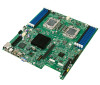
Intel® Server Board S5500WB TPS List of Figures List of Figures Figure 1. Intel® Server Board S5500WB 12V 4 Figure 2. Intel Server Board S5500WB SSI 5 Figure 3. Intel® Server Board S5500WB Components (both SKUs are shown 6 Figure 4. Rear Panel Connector Placement 8 Figure 5. Baseboard and Mounting holes 9 Figure 6. Connector Locations 10 Figure 7. Primary Side Height Restrictions 11 Figure 8. Secondary Side Height Restrictions 12 Figure 9. Intel® Server Board S5500WB Functional Block Diagram 14 Figure 10. Lifting the load lever of ILM cover 17 Figure 11. Removing the socket cover 17 Figure 12. Installing processor 18 Figure 13. Package Installation/Remove Feature 19 Figure 14. Installing/Removing Heatsink 20 Figure 15. Intel® QPI Link...20 Figure 16. Memory Channel Population 23 Figure 17. Installing Memory...24 Figure 18. Mirroring Memory Configuration 26 Figure 19. Integrated BMC Hardware 33 Figure 20. S5500WB I2C\SMBUS Block Diagram 44 Figure 21: Jumper Blocks (J1B5, J1C2, J1C3, J1B4, J6A3, J6A2, J7A2 46 Figure 22: 5-V Standby Status LED Location 68 Figure 23. Fan Fault LED Locations 69 Figure 24. System Status LED Location 70 Figure 25. DIMM Fault LEDs Locations 73 Figure 26. Rear Panel Diagnostic LEDs 74 Figure 27: Thermal Zones...76 Figure 28: Location of Fan Connectors 77 Figure 29. Fans and Sensors Block Diagram 78 Figure 30: Temp Sensor Location 80 Figure 31. Unified Retention System and Unified Backplate Assembly 81 Revision 1.9 ix Intel order number E53971-008

  • 1
  • 2
  • 3
  • 4
  • 5
  • 6
  • 7
  • 8
  • 9
  • 10
  • 11
  • 12
  • 13
  • 14
  • 15
  • 16
  • 17
  • 18
  • 19
  • 20
  • 21
  • 22
  • 23
  • 24
  • 25
  • 26
  • 27
  • 28
  • 29
  • 30
  • 31
  • 32
  • 33
  • 34
  • 35
  • 36
  • 37
  • 38
  • 39
  • 40
  • 41
  • 42
  • 43
  • 44
  • 45
  • 46
  • 47
  • 48
  • 49
  • 50
  • 51
  • 52
  • 53
  • 54
  • 55
  • 56
  • 57
  • 58
  • 59
  • 60
  • 61
  • 62
  • 63
  • 64
  • 65
  • 66
  • 67
  • 68
  • 69
  • 70
  • 71
  • 72
  • 73
  • 74
  • 75
  • 76
  • 77
  • 78
  • 79
  • 80
  • 81
  • 82
  • 83
  • 84
  • 85
  • 86
  • 87
  • 88
  • 89
  • 90
  • 91
  • 92
  • 93
  • 94
  • 95
  • 96
  • 97
  • 98
  • 99
  • 100
  • 101
  • 102
  • 103
  • 104
  • 105
  • 106
  • 107
  • 108
  • 109
  • 110
  • 111
  • 112
  • 113
  • 114
  • 115
  • 116
  • 117

Intel® Server Board S5500WB TPS
List of Figures
Revision 1.9
Intel order number E53971-008
ix
List of Figures
Figure 1. Intel
®
Server Board S5500WB 12V
..............................................................................
4
Figure 2. Intel Server Board S5500WB SSI
................................................................................
5
Figure 3. Intel
®
Server Board S5500WB Components (both SKUs are shown)
...........................
6
Figure 4. Rear Panel Connector Placement:
...............................................................................
8
Figure 5. Baseboard and Mounting holes
....................................................................................
9
Figure 6. Connector Locations
..................................................................................................
10
Figure 7. Primary Side Height Restrictions
................................................................................
11
Figure 8. Secondary Side Height Restrictions
...........................................................................
12
Figure 9. Intel
®
Server Board S5500WB Functional Block Diagram
..........................................
14
Figure 10. Lifting the load lever of ILM cover
............................................................................
17
Figure 11. Removing the socket cover
......................................................................................
17
Figure 12. Installing processor
..................................................................................................
18
Figure 13. Package Installation/Remove Feature
.....................................................................
19
Figure 14. Installing/Removing Heatsink
...................................................................................
20
Figure 15. Intel
®
QPI Link
..........................................................................................................
20
Figure 16. Memory Channel Population
....................................................................................
23
Figure 17. Installing Memory
.....................................................................................................
24
Figure 18. Mirroring Memory Configuration
...............................................................................
26
Figure 19. Integrated BMC Hardware
.......................................................................................
33
Figure 20. S5500WB I2C\SMBUS Block Diagram
....................................................................
44
Figure 21: Jumper Blocks (J1B5, J1C2, J1C3, J1B4, J6A3, J6A2, J7A2)
.................................
46
Figure 22: 5-V Standby Status LED Location
............................................................................
68
Figure 23. Fan Fault LED Locations
..........................................................................................
69
Figure 24. System Status LED Location
...................................................................................
70
Figure 25. DIMM Fault LEDs Locations
.....................................................................................
73
Figure 26. Rear Panel Diagnostic LEDs
....................................................................................
74
Figure 27: Thermal Zones
.........................................................................................................
76
Figure 28: Location of Fan Connectors
.....................................................................................
77
Figure 29. Fans and Sensors Block Diagram
............................................................................
78
Figure 30: Temp Sensor Location
.............................................................................................
80
Figure 31. Unified Retention System and Unified Backplate Assembly
.....................................
81