Fujitsu MHN2150AT Manual/User Guide - Page 190
C141-e120-02en, Mode 0, In Ns, Comment
 |
View all Fujitsu MHN2150AT manuals
Add to My Manuals
Save this manual to your list of manuals |
Page 190 highlights
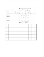
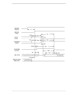
Interface 5.6.3.2 Ultra DMA data burst timing requirements Table 5.18 Ultra DMA data burst timing requirements (1 of 2) NAME MODE 0 MODE 1 MODE 2 MODE 3 MODE 4 MODE 5 (in ns) (in ns) (in ns) (in ns) (in ns) (in ns) COMMENT MIN MAX MIN MAX MIN MAX MIN MAX MIN MAX MIN MAX t2CYCTYP 240 160 120 90 tCYC 112 73 54 39 t2CYC 230 153 115 86 tDS 15 10 7 7 tDH 5 5 5 5 60 40 Typical sustained average two cycle time 25 16.8 Cycle time allowing for asymmetry and clock variations (from STROBE edge to STROBE edge) 57 38 Two cycle time allowing for clock variations (from rising edge to next rising edge or from falling edge to next falling edge of STROBE) 5 4 Data setup time at recipient (from data valid until STROBE edge) (*2), (*5) 5 4.6 Data hold time at recipient (from STROBE edge until data may become invalid) (*2), (*5) tDVS tDVH tCS tCH tCVS tCVH t ZFS t DZFS t FS 70 48 31 20 6.7 4.8 6.2 6.2 6.2 6.2 6.2 4.8 15 10 7 7 5 5 5 5 5 5 5 5 70 48 31 20 6.7 10 6.2 6.2 6.2 6.2 6.2 10 0 0 0 0 0 35 70 48 31 20 6.7 25 230 200 170 130 120 Data valid setup time at sender (from data valid until STROBE edge) (*3) Data valid hold time at sender (from STROBE edge until data may become invalid) (*3) CRC word setup time at device (*2) CRC word hold time device (*2) CRC word valid setup time at host (from CRC valid until DMACK-negation) (*3) CRC word valid hold time at sender (from DMACK-negation until CRC may become invalid) (*3) Time from STROBE output released-to-driving until the first transition of critical timing Time from data output releasedto-driving until the first transition of critical timing 90 First STROBE time (for device to first negate DSTROBE from STOP during a data in burst) 5-114 C141-E120-02EN
-
 1
1 -
2
-
3
-
4
-
5
-
6
-
7
-
8
-
9
-
10
-
11
-
12
-
13
-
14
-
15
-
16
-
17
-
18
-
19
-
20
-
21
-
22
-
23
-
24
-
25
-
26
-
27
-
28
-
29
-
30
-
31
-
32
-
33
-
34
-
35
-
36
-
37
-
38
-
39
-
40
-
41
-
42
-
43
-
44
-
45
-
46
-
47
-
48
-
49
-
50
-
51
-
52
-
53
-
54
-
55
-
56
-
57
-
58
-
59
-
60
-
61
-
62
-
63
-
64
-
65
-
66
-
67
-
68
-
69
-
70
-
71
-
72
-
73
-
74
-
75
-
76
-
77
-
78
-
79
-
80
-
81
-
82
-
83
-
84
-
85
-
86
-
87
-
88
-
89
-
90
-
91
-
92
-
93
-
94
-
95
-
96
-
97
-
98
-
99
-
100
-
101
-
102
-
103
-
104
-
105
-
106
-
107
-
108
-
109
-
110
-
111
-
112
-
113
-
114
-
115
-
116
-
117
-
118
-
119
-
120
-
121
-
122
-
123
-
124
-
125
-
126
-
127
-
128
-
129
-
130
-
131
-
132
-
133
-
134
-
135
-
136
-
137
-
138
-
139
-
140
-
141
-
142
-
143
-
144
-
145
-
146
-
147
-
148
-
149
-
150
-
151
-
152
-
153
-
154
-
155
-
156
-
157
-
158
-
159
-
160
-
161
-
162
-
163
-
164
-
165
-
166
-
167
-
168
-
169
-
170
-
171
-
172
-
173
-
174
-
175
-
176
-
177
-
178
-
179
-
180
-
181
-
182
-
183
-
184
-
 185
185 -
 186
186 -
 187
187 -
 188
188 -
 189
189 -
 190
190 -
 191
191 -
 192
192 -
 193
193 -
 194
194 -
 195
195 -
196
-
197
-
198
-
199
-
200
-
201
-
202
-
203
-
204
-
205
-
206
-
207
-
208
-
209
-
210
-
211
-
212
-
213
-
214
-
215
-
216
-
217
-
218
-
219
-
220
-
221
-
222
-
223
-
224
-
225
-
226
-
227
-
228
-
229
-
230
-
231
-
232
-
233
-
234
-
235
-
236
 |
 |
