Sharp GX30 Service Manual - Page 129
SD interface clock SD_CLK, UART_RTS for Bluetooth module
 |
View all Sharp GX30 manuals
Add to My Manuals
Save this manual to your list of manuals |
Page 129 highlights
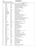
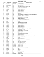
Pin No. 64 65 66 67 68 69 70 71 72 73 74 75 76 77 78 79 80 81 82 83 84 85 86 87 88 89 90 91 92 93 94 95 96 97 98 99 100 101 102 103 104 105 106 107 108 109 110 111 112 113 114 115 116 117 118 119 120 121 122 123 124 125 126 127 Terminal name MC_DAT[1] GND VEXT KEYPADCOL[0] VEXT GPIO_15 GPIO_16 ADD[13] ADD[12] ADD[8] ADD[6] GPO_22 GPIO_14 GPIO_10 GPIO_12 VMEM ADD[14] GND VCC ADD[10] CLKOUT MC_DAT[3] GND GND GPIO_13 GPIO_7 GPIO_9 ADD[19] ADD[17] ADD[18] ADD[15] ADD[16] CSFS MC_CLK VCC GPIO_11 GPIO_8 GPIO_5 GPIO_6 ADD[22] ADD[21] GPIO_40 ADD[20] GND ADD[23] GND VEXT GND GPIO_4 GPIO_2 GPIO_3 DATA[2] DATA[0] DATA[5] DATA[1] DATA[3] VCC DMINUS GPIO_18 GND GPIO_1 USC[5] GPIO_0 DATA[4] Input/Output Input/Output - Input Output Input Input Output Output Output Output Output Output Output Input Output Input Output - Input Output Output Input/Output - - Input Input Input Output Output Output Output Output Output Input Input Input Input Input Input Output Output Output Output - Output - Input - Output Output Input Input/Output Input/Output Input/Output Input/Output Input/Output Input Input Output - Input Input Output Input/Output CONFIDENTIAL Description of terminal SD interface data bus 1 Ground System interface power supply 2.4 - 3.3 V (VINT) KEYIN signal output 0 System interface power supply 2.4 - 3.3 V (VINT) PCM data input for Bluetooth module PCM SYNC output for Bluetooth module Processor address bus 13 Processor address bus 12 Processor address bus 8 Processor address bus 6 VPP control for flash memory 1 PCM clock output for Bluetooth module USB detection Reset output for main LCD controller/Sub LCD driver/Power management IC Memory power supply 2.7 - 3.3 V (VMEM) Processor address bus 14 Ground Core power supply 1.7 - 1.9 V (VCORE) Processor address bus 10 13 MHz clock output for analog BB (CLKOUT) SD interface data bus 3 Ground Ground Interrupt input from camera module Hands free kit (earphone) detection Manufacturer specific input from I/O connector Processor address bus 19 Processor address bus 17 Processor address bus 18 Processor address bus 15 Processor address bus 16 Control serial port framing signal output to analog BB SD interface clock (SD_CLK) Core power supply 1.7 - 1.9 V (VCORE) Flip switch detection Stereo/monaural detection for hands free kit (earphone) SD card detection Interrupt input from main LCD controller Processor address bus 22 Processor address bus 21 13 MHz clock output for main LCD controller & Sound generator IC Processor address bus 20 Ground Processor address bus 23 Ground System interface power supply 2.4 - 3.3 V (VINT) Ground UART_CTS for Bluetooth module USB charge current control UART_RTS for Bluetooth module Processor data bus 2 Processor data bus 0 Processor data bus 5 Processor data bus 1 Processor data bus 3 Core power supply 1.7 - 1.9 V (VCORE) USB DJTAG TCK Ground IrDA receive data USC pin (CTS/Ginie_TX) IrDA transmit data Processor data bus 4 6 - 9 GX30
-
 1
1 -
2
-
3
-
4
-
5
-
6
-
7
-
8
-
9
-
10
-
11
-
12
-
13
-
14
-
15
-
16
-
17
-
18
-
19
-
20
-
21
-
22
-
23
-
24
-
25
-
26
-
27
-
28
-
29
-
30
-
31
-
32
-
33
-
34
-
35
-
36
-
37
-
38
-
39
-
40
-
41
-
42
-
43
-
44
-
45
-
46
-
47
-
48
-
49
-
50
-
51
-
52
-
53
-
54
-
55
-
56
-
57
-
58
-
59
-
60
-
61
-
62
-
63
-
64
-
65
-
66
-
67
-
68
-
69
-
70
-
71
-
72
-
73
-
74
-
75
-
76
-
77
-
78
-
79
-
80
-
81
-
82
-
83
-
84
-
85
-
86
-
87
-
88
-
89
-
90
-
91
-
92
-
93
-
94
-
95
-
96
-
97
-
98
-
99
-
100
-
101
-
102
-
103
-
104
-
105
-
106
-
107
-
108
-
109
-
110
-
111
-
112
-
113
-
114
-
115
-
116
-
117
-
118
-
119
-
120
-
121
-
122
-
123
-
 124
124 -
 125
125 -
 126
126 -
 127
127 -
 128
128 -
 129
129 -
 130
130 -
 131
131 -
 132
132 -
 133
133 -
 134
134 -
135
-
136
-
137
-
138
-
139
-
140
-
141
-
142
-
143
-
144
-
145
-
146
-
147
-
148
-
149
-
150
-
151
-
152
-
153
-
154
-
155
-
156
-
157
-
158
-
159
-
160
-
161
-
162
-
163
-
164
-
165
-
166
 |
 |
