Sharp GX30 Service Manual - Page 131
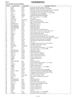
IC108 VHIR3112Q26-1L R3112Q261A: VOLTAGE DETECTOR, Pin No., Terminal name, Input/Output
 |
View all Sharp GX30 manuals
Add to My Manuals
Save this manual to your list of manuals |
Page 131 highlights
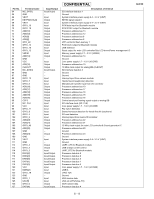
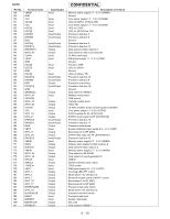
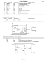
CONFIDENTIAL Pin No. 192 193 194 195 196 197 198 199 200 201 202 203 204 Terminal name NAUXCS1 GPIO_43 VDDUSB GPIO_23 SIMDATAIO GPIO_24 GPIO_19 GPIO_21 GPO_2 GND GPO_8 GPO_9 GPO_10 Input/Output Output Output Input Output Input/Output Output Output Output Output - Output Output Output Description of terminal Command latch enable for flash memory 2 Chip select for Camera module USB power supply 2.8 - 3.3 V (VUSB) SIM interface reset SIM interface data input/output Sound generator IC reset JTAG TMS JTAG TDO Write protect control for flash memory 1 Ground IrDA power ON/OFF control Band select 3 for RF (BS3) BUF OFF for main LCD controller In this unit, the terminal with asterisk mark (*) is (open) terminal which is not connected to the outside. IC107 VHIEW6671++-1R (EW6671): HALL Pin No. 1 2 3 Terminal name VDD GND OUT Input/Output Input - Output Input Ground Output Description of terminal VDD 1 Pulse Regulator Reg. 3 Amplifier Output stage 3 OUTPUT Hall cell Schmitt trigger & Latch 2 GND 1 2 IC108 VHIR3112Q26-1L (R3112Q261A): VOLTAGE DETECTOR Pin No. 1 2 3 4 Terminal name VDD GND CD OUT Input/Output - - Input Output Description of terminal Power supply Ground External condenser connection terminal for delay Output terminal (L: when output is detected, H: when output is canceled) VDD 1 RD + - VREF 3 CD 4 OUT 2 GND GX30 6 - 11
-
 1
1 -
2
-
3
-
4
-
5
-
6
-
7
-
8
-
9
-
10
-
11
-
12
-
13
-
14
-
15
-
16
-
17
-
18
-
19
-
20
-
21
-
22
-
23
-
24
-
25
-
26
-
27
-
28
-
29
-
30
-
31
-
32
-
33
-
34
-
35
-
36
-
37
-
38
-
39
-
40
-
41
-
42
-
43
-
44
-
45
-
46
-
47
-
48
-
49
-
50
-
51
-
52
-
53
-
54
-
55
-
56
-
57
-
58
-
59
-
60
-
61
-
62
-
63
-
64
-
65
-
66
-
67
-
68
-
69
-
70
-
71
-
72
-
73
-
74
-
75
-
76
-
77
-
78
-
79
-
80
-
81
-
82
-
83
-
84
-
85
-
86
-
87
-
88
-
89
-
90
-
91
-
92
-
93
-
94
-
95
-
96
-
97
-
98
-
99
-
100
-
101
-
102
-
103
-
104
-
105
-
106
-
107
-
108
-
109
-
110
-
111
-
112
-
113
-
114
-
115
-
116
-
117
-
118
-
119
-
120
-
121
-
122
-
123
-
124
-
125
-
 126
126 -
 127
127 -
 128
128 -
 129
129 -
 130
130 -
 131
131 -
 132
132 -
 133
133 -
 134
134 -
 135
135 -
 136
136 -
137
-
138
-
139
-
140
-
141
-
142
-
143
-
144
-
145
-
146
-
147
-
148
-
149
-
150
-
151
-
152
-
153
-
154
-
155
-
156
-
157
-
158
-
159
-
160
-
161
-
162
-
163
-
164
-
165
-
166
 |
 |
