Sharp GX30 Service Manual - Page 130
Band select 2 for RF BS2
 |
View all Sharp GX30 manuals
Add to My Manuals
Save this manual to your list of manuals |
Page 130 highlights
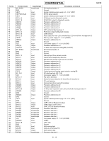
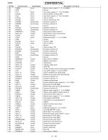
GX30 Pin No. 128 129 130 131 132 133 134 135 136 137 138 139 140 141 142 143 144 145 146 147 148 149 150 151 152 153 154 155 156 157 158 159 160 161 162 163 164 165 166 167 168 169 170 171 172 173 174 175 176 177 178 179 180 181 182 183 184 185 186 187 188 189 190* 191 Terminal name VMEM GND VCC USC[6] VCC USC[2] USC[4] DATA[7] DATA[6] GND DATA[9] DATA[13] NROMCS1 GPIO_42 CLKIN VSIM GND USC[3] USC[1] GND USC[0] DATA[10] DATA[8] NRD DATA[14] GND NRAMCS2 GPIO_44 VSSUSB GPIO_47 GPIO_20 CLKON VCC GPO_18 GPO_21 DATA[12] DATA[11] NWE VEXT GPO_11 GPO_20 DATA[15] VMEM NADV NGPCS1 VMEM GPIO_45 GPIO_46 DPLUS SIMCLK JTAGEN VEXT GPO_3 GPO_4 GPO_7 GPO_16 GPO_17 NHWR/NUSB GPO_19 NLWR/NLSB NWAIT NRESET BURSTCLK NRAMCS1 Input/Output Input - Input Input Input Input Input Input/Output Input/Output - Input/Output Input/Output Output Output Input Input - Input Input - Input Input/Output Input/Output Output Input/Output - Output Input - Output Output Output Input Output Output Input/Output Input/Output Output Input Output Output Input/Output Input Output Output Input Output Output Input Output Input Input Output Output Output Output Output Output Output Output Input Input Output Output CONFIDENTIAL Description of terminal Memory power supply 2.7 - 3.3 V (VMEM) Ground Core power supply 1.7 - 1.9 V (VCORE) USC pin (GPIO_31/Ginie_RX) Core power supply 1.7 - 1.9 V (VCORE) USC pin (TXD) USC pin (RTS/Ginie_RX) Processor data bus 7 Processor data bus 6 Ground Processor data bus 9 Processor data bus 13 Chip select for flash memory 1 Chip select for main LCD controller 13 MHz clock input SIM power supply 1.7 - 3.3 V (VSIM) Ground Pull up to VINT USC pin (RXD) Ground USC pin (Ginie_TX) Processor data bus 10 Processor data bus 8 Processor read strobe Processor data bus 14 Ground Chip select for SRAM 2 Wakeup mode select USB ground Camera module reset JTAG TDI 13 MHz oscillator power control signal (VCXOEN) Core power supply 1.7-1.9V (VCORE) SYNTH enable for RF (SYNTHEN) SYNTH clock output for RF (SYNTHCLK) Processor data bus 12 Processor data bus 11 Processor write strobe System interface power supply 2.4 - 3.3 V (VINT) Band select 4 for RF (BS4) SYNTH data output for RF (SYNTHDATA) Processor data bus 15 Memory power supply 2.7 - 3.3 V (VMEM) Address latch enable for flash memory 2 Chip select for flash memory 2 Memory power supply 2.7 - 3.3 V (VMEM) Chip select for 4M SRAM Chip select for sound generator IC USB D+ System interface clock output JTAG enable SIM power supply 2.4 - 3.3 V (VINT) Incoming LED OFF control Mode select 1 for interface IC Bluetooth module power ON/OFF control Band select 1 for RF (BS1) Band select 2 for RF (BS2) Processor high write strobe Mode select 3 for interface IC Processor low write strobe Processor wait input System reset input Not used Chip select for SRAM 1 6 - 10
-
 1
1 -
2
-
3
-
4
-
5
-
6
-
7
-
8
-
9
-
10
-
11
-
12
-
13
-
14
-
15
-
16
-
17
-
18
-
19
-
20
-
21
-
22
-
23
-
24
-
25
-
26
-
27
-
28
-
29
-
30
-
31
-
32
-
33
-
34
-
35
-
36
-
37
-
38
-
39
-
40
-
41
-
42
-
43
-
44
-
45
-
46
-
47
-
48
-
49
-
50
-
51
-
52
-
53
-
54
-
55
-
56
-
57
-
58
-
59
-
60
-
61
-
62
-
63
-
64
-
65
-
66
-
67
-
68
-
69
-
70
-
71
-
72
-
73
-
74
-
75
-
76
-
77
-
78
-
79
-
80
-
81
-
82
-
83
-
84
-
85
-
86
-
87
-
88
-
89
-
90
-
91
-
92
-
93
-
94
-
95
-
96
-
97
-
98
-
99
-
100
-
101
-
102
-
103
-
104
-
105
-
106
-
107
-
108
-
109
-
110
-
111
-
112
-
113
-
114
-
115
-
116
-
117
-
118
-
119
-
120
-
121
-
122
-
123
-
124
-
 125
125 -
 126
126 -
 127
127 -
 128
128 -
 129
129 -
 130
130 -
 131
131 -
 132
132 -
 133
133 -
 134
134 -
 135
135 -
136
-
137
-
138
-
139
-
140
-
141
-
142
-
143
-
144
-
145
-
146
-
147
-
148
-
149
-
150
-
151
-
152
-
153
-
154
-
155
-
156
-
157
-
158
-
159
-
160
-
161
-
162
-
163
-
164
-
165
-
166
 |
 |
