Epson ActionPrinter 3250 User Manual - Page 77
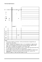
Appendix A-9, Pulled up to 5V through 1 .O KQ
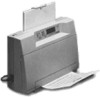 |
View all Epson ActionPrinter 3250 manuals
Add to My Manuals
Save this manual to your list of manuals |
Page 77 highlights
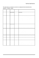
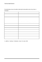
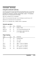
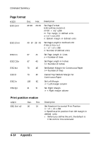
Technical Specifications The table below provides the connector pin assignments and describes their respective interface signals. Signal Return Signal Direction Pin Pin Description 1 19 STROBE IN STROBE pulse to read data. Pulse width must be more than 0.5 microseconds at the receiving terminal. 2 20 DATA 1 IN These signals represent information of 3 21 DATA 2 IN the 1st to 8th bits of parallel data, 4 22 DATA 3 IN respectively. Each signal is at HIGH level 5 23 DATA 4 IN when data is logical 1 and LOW when 6 24 DATA 5 IN it is logical 0. 7 25 DATA 6 IN 8 26 DATA 7 IN 9 27 DATA8 IN 10 28 ACKNLG OUT About a IO-microsecond pulse. LOW indicates that data has been received and that the printer is ready to accept more data. 11 29 BUSY OUT A HIGH signal indicates the printer cannot receive data. The signal goes HIGH in the following cases: 1) During data entry (ea. char. time) 2) During printing 3) During an error state 12 30 PE OUT A HIGH signal indicates that the printer is in a paper-out state or in an error state. 13 - SLCT OUT Pulled up to 5V through 1 .O KQ resistance. 14 - AUTO FEED XT IN When this signal is LOW, the paper is automatically fed one line after printing. (The signal level can be fixed to this by setting Auto Line Feed to on in the default-setting mode.) Appendix A-9
-
 1
1 -
2
-
3
-
4
-
5
-
6
-
7
-
8
-
9
-
10
-
11
-
12
-
13
-
14
-
15
-
16
-
17
-
18
-
19
-
20
-
21
-
22
-
23
-
24
-
25
-
26
-
27
-
28
-
29
-
30
-
31
-
32
-
33
-
34
-
35
-
36
-
37
-
38
-
39
-
40
-
41
-
42
-
43
-
44
-
45
-
46
-
47
-
48
-
49
-
50
-
51
-
52
-
53
-
54
-
55
-
56
-
57
-
58
-
59
-
60
-
61
-
62
-
63
-
64
-
65
-
66
-
67
-
68
-
69
-
70
-
71
-
 72
72 -
 73
73 -
 74
74 -
 75
75 -
 76
76 -
 77
77 -
 78
78 -
 79
79 -
 80
80 -
 81
81 -
 82
82 -
83
-
84
-
85
-
86
-
87
-
88
-
89
-
90
-
91
-
92
-
93
-
94
-
95
-
96
-
97
-
98
-
99
-
100
-
101
-
102
-
103
 |
 |
