Hitachi IC25N040ATCS04-0 Specifications - Page 80
Registers
 |
UPC - 683728198664
View all Hitachi IC25N040ATCS04-0 manuals
Add to My Manuals
Save this manual to your list of manuals |
Page 80 highlights
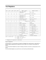
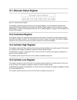
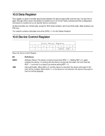
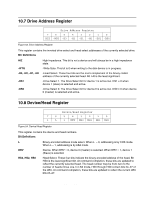
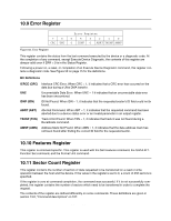
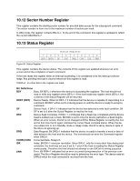
10.0 Registers Addresses Functions CS0- CS1- DA2 DA1 DA0 READ (DIOR-) Data bus high N N x x x impedance WRITE (DIOW-) Not used Control block registers Data bus high N A 0 x x impedance Data bus high N A 1 0 x impedance N A 1 1 0 Alternate Status N A 1 1 1 Device Address Not used Not used Device Control Not used Command block registers A N 0 A N 0 A N 0 A N 0 A N 0 A N 1 A N 1 A N 1 A N 1 A N 1 A N 1 A N 1 A A x Logic conventions: 0 0 Data 0 1 Error Register 1 0 Sector Count 1 1 Sector Number 1 1 * LBA bits 0-7 0 0 Cylinder Low 0 0 * LBA bits 8-15 0 1 Cylinder High 0 1 * LBA bits 16-23 1 0 Device/Head. 1 0 * LBA bits 24-27 1 1 Status x x Invalid address A = signal asserted N = signal not asserted x = either A or N Data Features Sector Count Sector Number * LBA bits 0-7 Cylinder Low * LBA bits 8-15 Cylinder High * LBA bits 16-23 Device/Head * LBA bits 24-27 Command Invalid address * = Mapping of registers in LBA mode Figure 50. Register Set Communication to or from the device is through an I/O Register that routes the input or output data to or from the registers addressed by the signals from the host (CS0-, CS1-, DA2, DA1, DA0, DIOR- and DIOW-). The Command Block Registers are used for sending commands to the device or posting status from the device. The Control Block Registers are used for device control and to post alternate status. Hitachi Travelstar 60GH & 40GN hard disk drive specifications 67
-
 1
1 -
2
-
3
-
4
-
5
-
6
-
7
-
8
-
9
-
10
-
11
-
12
-
13
-
14
-
15
-
16
-
17
-
18
-
19
-
20
-
21
-
22
-
23
-
24
-
25
-
26
-
27
-
28
-
29
-
30
-
31
-
32
-
33
-
34
-
35
-
36
-
37
-
38
-
39
-
40
-
41
-
42
-
43
-
44
-
45
-
46
-
47
-
48
-
49
-
50
-
51
-
52
-
53
-
54
-
55
-
56
-
57
-
58
-
59
-
60
-
61
-
62
-
63
-
64
-
65
-
66
-
67
-
68
-
69
-
70
-
71
-
72
-
73
-
74
-
 75
75 -
 76
76 -
 77
77 -
 78
78 -
 79
79 -
 80
80 -
 81
81 -
 82
82 -
 83
83 -
 84
84 -
 85
85 -
86
-
87
-
88
-
89
-
90
-
91
-
92
-
93
-
94
-
95
-
96
-
97
-
98
-
99
-
100
-
101
-
102
-
103
-
104
-
105
-
106
-
107
-
108
-
109
-
110
-
111
-
112
-
113
-
114
-
115
-
116
-
117
-
118
-
119
-
120
-
121
-
122
-
123
-
124
-
125
-
126
-
127
-
128
-
129
-
130
-
131
-
132
-
133
-
134
-
135
-
136
-
137
-
138
-
139
-
140
-
141
-
142
-
143
-
144
-
145
-
146
-
147
-
148
-
149
-
150
-
151
-
152
-
153
-
154
-
155
-
156
-
157
-
158
-
159
-
160
-
161
-
162
-
163
-
164
-
165
-
166
-
167
-
168
-
169
-
170
-
171
-
172
-
173
-
174
-
175
-
176
-
177
-
178
-
179
-
180
-
181
-
182
-
183
-
184
-
185
-
186
-
187
-
188
-
189
-
190
-
191
-
192
-
193
-
194
-
195
-
196
-
197
-
198
-
199
-
200
-
201
-
202
-
203
-
204
-
205
-
206
-
207
-
208
-
209
-
210
-
211
-
212
-
213
-
214
-
215
-
216
-
217
 |
 |
