Intel D101GGC Product Specification - Page 11
Block Diagram - vga
 |
View all Intel D101GGC manuals
Add to My Manuals
Save this manual to your list of manuals |
Page 11 highlights
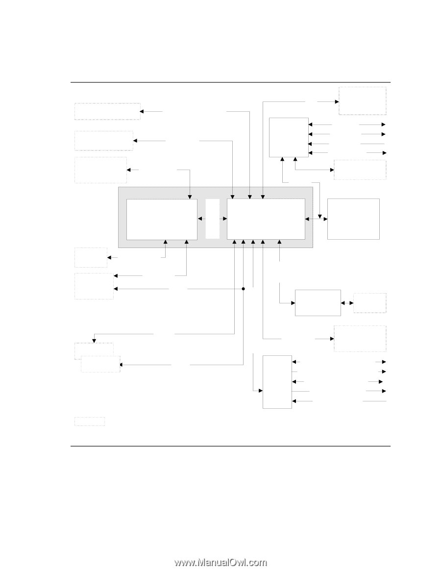
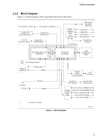
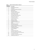
Product Description 1.1.2 Block Diagram Figure 1 is a block diagram of the major functional areas of the board. PCI Express x1 Slot 1 PCI Express x1 Interface Parallel ATA IDE Connectors (2) Parallel ATA IDE Interface LGA775 Processor Socket System Bus (800/533 MHz) USB Back Panel/ Front Panel USB Ports SMSC SCH5017 Legacy I/O Controller LPC Bus Serial Port Parallel Port PS/2 Mouse PS/2 Keyboard Diskette Drive Connector PCI Express x4 Interface High Definition Audio Link PCI Bus ATI Radeon Xpress 200 Northbridge ATI IXP 450 Southbridge 4 Mbit Firmware Hub (FWH) VGA Port Display Interface Channel A DIMMs (2) Memory Bus SMBus Realtek 8101L LAN Controller LAN Connector PCI Slot 1 PCI Slot 2 PCI Bus SMBus Serial ATA IDE Interface Serial ATA IDE Connectors (4) Realtek ALC861 Audio Codec Line In or Rear Left/Right Out Line Out or Front Left/Right Out Mic In or Center/LFE Out Line Out [Front Panel] Mic In [Front Panel] = connector or socket Figure 1. Block Diagram OM18245 11
-
 1
1 -
2
-
3
-
4
-
5
-
 6
6 -
 7
7 -
 8
8 -
 9
9 -
 10
10 -
 11
11 -
 12
12 -
 13
13 -
 14
14 -
 15
15 -
 16
16 -
17
-
18
-
19
-
20
-
21
-
22
-
23
-
24
-
25
-
26
-
27
-
28
-
29
-
30
-
31
-
32
-
33
-
34
-
35
-
36
-
37
-
38
-
39
-
40
-
41
-
42
-
43
-
44
-
45
-
46
-
47
-
48
-
49
-
50
-
51
-
52
-
53
-
54
-
55
-
56
-
57
-
58
-
59
-
60
-
61
-
62
-
63
-
64
-
65
-
66
-
67
-
68
-
69
-
70
-
71
-
72
-
73
-
74
 |
 |