Intel D848PMB Technical Product Specification - Page 15
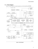
Block Diagram
 |
View all Intel D848PMB manuals
Add to My Manuals
Save this manual to your list of manuals |
Page 15 highlights
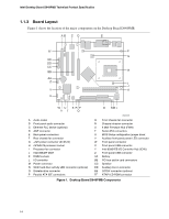
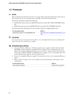
Product Description 1.1.4 Block Diagram Figure 2 is a block diagram of the major functional areas of the Desktop Board D848PMB. = connector or socket Parallel ATA IDE Connectors (2) Parallel ATA IDE Interface mPGA478 System Bus Processor Socket (400/533/800 MHz) LAN Connector Gigabit LAN PLC (Optional) CSA Interface AGP Interface Universal 0.8/ 1.5 V AGP 3.0 Connector Intel 82848P Memory Controller Hub (MCH) AHA Bus USB LPC Bus I/O Controller LPC Bus Intel 82801EB I/O Controller Hub (ICH5) Back Panel/ Front Panel USB Ports Serial Port Parallel Port PS/2 Mouse PS/2 Keyboard Diskette Drive Connector 4 Mbit Firmware Hub (FWH) DIMM Sockets (2) Memory Bus SMBus PCI Bus PCI Slot 1 PCI Slot 2 PCI Slot 3 SMBus Hardware Monitoring and Fan Control ASIC Line In Line Out Mic In Auxiliary Line In CD-ROM Realtek ALC202A Audio Codec (Optional) AC Link CSMA/CD Unit Interface 10/100 LAN PLC (Optional) LAN Connector AC Serial ATA Link IDE Interface Serial ATA IDE Connectors (2) AD1985 Audio Codec (Optional) Front Left and Right Out Center and LFE Out Rear Left and Right Out S/PDIF Line In Mic In CD-ROM Auxiliary Line In Figure 2. Block Diagram OM16508 15
-
 1
1 -
2
-
3
-
4
-
5
-
6
-
7
-
8
-
9
-
 10
10 -
 11
11 -
 12
12 -
 13
13 -
 14
14 -
 15
15 -
 16
16 -
 17
17 -
 18
18 -
 19
19 -
 20
20 -
21
-
22
-
23
-
24
-
25
-
26
-
27
-
28
-
29
-
30
-
31
-
32
-
33
-
34
-
35
-
36
-
37
-
38
-
39
-
40
-
41
-
42
-
43
-
44
-
45
-
46
-
47
-
48
-
49
-
50
-
51
-
52
-
53
-
54
-
55
-
56
-
57
-
58
-
59
-
60
-
61
-
62
-
63
-
64
-
65
-
66
-
67
-
68
-
69
-
70
-
71
-
72
-
73
-
74
-
75
-
76
-
77
-
78
-
79
-
80
-
81
-
82
-
83
-
84
-
85
-
86
-
87
-
88
-
89
-
90
-
91
-
92
-
93
-
94
-
95
-
96
-
97
-
98
-
99
-
100
-
101
-
102
-
103
-
104
-
105
-
106
-
107
-
108
-
109
-
110
-
111
-
112
-
113
-
114
-
115
-
116
-
117
-
118
-
119
-
120
-
121
-
122
 |
 |
