Intel S3420GPLC Product Specification - Page 113
Common Mode Noise, Ripple/Noise, Timing Requirements
 |
UPC - 735858211819
View all Intel S3420GPLC manuals
Add to My Manuals
Save this manual to your list of manuals |
Page 113 highlights
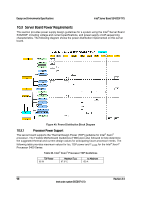
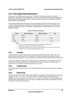
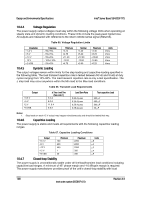
Intel® Server Board S3420GP TPS Design and Environmental Specifications sensing through the submission of Bode plots. Closed-loop stability is ensured at the maximum and minimum loads as applicable. 10.4.8 Common Mode Noise The Common Mode noise on any output does not exceed 350 mV pk-pk over the frequency band of 10 Hz to 20 MHz. The measurement is made across a 100Ω resistor between each of the DC outputs, including ground, at the DC power connector and chassis ground (power subsystem enclosure). The test setup uses a FET probe such as Tektronix* model P6046 or equivalent. 10.4.9 Ripple/Noise The maximum allowed ripple/noise output of the power supply is defined in the following table. This is measured over a bandwidth of 0 Hz to 20 MHz at the power supply output connectors. A 10 F tantalum capacitor is placed in parallel with a 0.1 F ceramic capacitor at the point of measurement. Table 68. Ripple and Noise +3.3 V 50 mVp-p +5 V 50 mVp-p +12 V 120 mVp-p -12 V 120 mVp-p +5 VSB 50 mVp-p 10.4.10 Timing Requirements The timing requirements for the power supply operation are as follows: The output voltages must rise from 10% to within regulation limits (Tvout_rise) within 5 ms to 70 ms, except for 5 VSB, in which case it is allowed to rise from 1.0 ms to 25 ms. The +3.3 V, +5 V, and +12 V output voltages should start to rise approximately at the same time. All outputs must rise monotonically. The +5 V output must be greater than the +3.3 V output during any point of the voltage rise. The +5 V output must never be greater than the +3.3 V output by more than 2.25 V. Each output voltage should reach regulation within 50 ms (Tvout_on) of each other when the power supply is turned on. Each output voltage should fall out of regulation within 400 msec (Tvout_off) of each other when the power supply is turned off. Figure 41 and Figure 42 shows the timing requirements for the power supply being turned on and off via the AC input with PSON held low and the PSON signal with the AC input applied. Table 69. Output Voltage Timing Item Tvout_rise Tvout_on Tvout_off Description Output voltage rise time from each main output. All main outputs must be within regulation of each other within this time. All main outputs must leave regulation within this time. Minimum 5.01 Maximum 701 50 700 Units Msec Msec Msec Revision 2.4 101 Intel order number E65697-010
-
 1
1 -
2
-
3
-
4
-
5
-
6
-
7
-
8
-
9
-
10
-
11
-
12
-
13
-
14
-
15
-
16
-
17
-
18
-
19
-
20
-
21
-
22
-
23
-
24
-
25
-
26
-
27
-
28
-
29
-
30
-
31
-
32
-
33
-
34
-
35
-
36
-
37
-
38
-
39
-
40
-
41
-
42
-
43
-
44
-
45
-
46
-
47
-
48
-
49
-
50
-
51
-
52
-
53
-
54
-
55
-
56
-
57
-
58
-
59
-
60
-
61
-
62
-
63
-
64
-
65
-
66
-
67
-
68
-
69
-
70
-
71
-
72
-
73
-
74
-
75
-
76
-
77
-
78
-
79
-
80
-
81
-
82
-
83
-
84
-
85
-
86
-
87
-
88
-
89
-
90
-
91
-
92
-
93
-
94
-
95
-
96
-
97
-
98
-
99
-
100
-
101
-
102
-
103
-
104
-
105
-
106
-
107
-
 108
108 -
 109
109 -
 110
110 -
 111
111 -
 112
112 -
 113
113 -
 114
114 -
 115
115 -
 116
116 -
 117
117 -
 118
118 -
119
-
120
-
121
-
122
-
123
-
124
-
125
-
126
-
127
-
128
-
129
-
130
-
131
-
132
-
133
-
134
-
135
-
136
-
137
-
138
-
139
-
140
-
141
-
142
-
143
-
144
 |
 |
