Intel S3420GPLC Product Specification - Page 96
Serial Port Connectors, USB Connector
 |
UPC - 735858211819
View all Intel S3420GPLC manuals
Add to My Manuals
Save this manual to your list of manuals |
Page 96 highlights
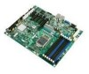
Connector/Header Locations and Pin-outs Intel® Server Board S3420GP TPS Pin Signal Name 45 P3V3 47 P3V3 49 P3V3 Pin 46 48 50 P3V3 P3V3 P3V3 Signal Name 7.5.5 Serial Port Connectors The server board provides one external DB9 Serial A port (J8A1) and one internal 9-pin serial B header (J1B2). The following tables define the pin-outs. Table 52. External Serial A Port Pin-out (J8A1) Pin Signal Name 1 SPA_DCD 2 SPA_SIN_L 3 SPA_SOUT_N 4 SPA_DTR 5 GND 6 SPA_DSR 7 SPA_RTS 8 SPA_CTS 9 SPA_RI 10 NC Description DCD (carrier detect) RXD (receive data) TXD (Transmit data) DTR (Data terminal ready) Ground DSR (data set ready) RTS (request to send) CTS (clear to send) RI (Ring Indicate) Table 53. Internal 9-pin Serial B Header Pin-out (J1B2) Pin Signal Name Description 1 SPB_DCD DCD (carrier detect) 2 SPB_DSR DSR (data set ready) 3 SPB_SIN_L RXD (receive data) 4 SPB_RTS RTS (request to send) 5 SPB_SOUT_N TXD (Transmit data) 6 SPB_CTS CTS (clear to send) 7 SPB_DTR DTR (Data terminal ready) 8 SPB_RI RI (Ring indicate) 9 SPB_EN_N Enable 10 NC 7.5.6 USB Connector There are four external USB ports on two NIC/USB combinations. Section 5.5.2 details the pinout of the connector. Two 2x5 connector on the server board (J1E1, J1D1) provides an option to support an additional USB port, each connector supporting two USB ports. The following table defines the pin-out of the connector. Table 54. Internal USB Connector Pin-out ( J1E1, J1D1) Pin Signal Name 1 USB2_VBUS4 2 USB2_VBUS5 Description USB power (port 4) USB power (port 5) 84 Revision 2.4 Intel order number E65697-010
-
 1
1 -
2
-
3
-
4
-
5
-
6
-
7
-
8
-
9
-
10
-
11
-
12
-
13
-
14
-
15
-
16
-
17
-
18
-
19
-
20
-
21
-
22
-
23
-
24
-
25
-
26
-
27
-
28
-
29
-
30
-
31
-
32
-
33
-
34
-
35
-
36
-
37
-
38
-
39
-
40
-
41
-
42
-
43
-
44
-
45
-
46
-
47
-
48
-
49
-
50
-
51
-
52
-
53
-
54
-
55
-
56
-
57
-
58
-
59
-
60
-
61
-
62
-
63
-
64
-
65
-
66
-
67
-
68
-
69
-
70
-
71
-
72
-
73
-
74
-
75
-
76
-
77
-
78
-
79
-
80
-
81
-
82
-
83
-
84
-
85
-
86
-
87
-
88
-
89
-
90
-
 91
91 -
 92
92 -
 93
93 -
 94
94 -
 95
95 -
 96
96 -
 97
97 -
 98
98 -
 99
99 -
 100
100 -
 101
101 -
102
-
103
-
104
-
105
-
106
-
107
-
108
-
109
-
110
-
111
-
112
-
113
-
114
-
115
-
116
-
117
-
118
-
119
-
120
-
121
-
122
-
123
-
124
-
125
-
126
-
127
-
128
-
129
-
130
-
131
-
132
-
133
-
134
-
135
-
136
-
137
-
138
-
139
-
140
-
141
-
142
-
143
-
144
 |
 |
