Intel S3420GPLC Product Specification - Page 95
pin PCI Express* Connector - raid configuration
 |
UPC - 735858211819
View all Intel S3420GPLC manuals
Add to My Manuals
Save this manual to your list of manuals |
Page 95 highlights
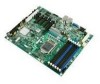
Intel® Server Board S3420GP TPS Connector/Header Locations and Pin-outs Pin 21 Signal Name LED_NIC1_2 Pin Signal Name 22 LED_NIC1_LINK1000_1 7.5.3 SATA The sever board provides up to six SATA connectors. The pin configuration for each connector is identical and defined in the following table. Table 50. SATA Connector Pin-out (J1H4, J1H1, J1G1, J1H3, J1G3, J1F4) Pin 1 2 3 4 5 6 7 Signal Name GND SATA/SAS_TX_P_C SATA/SAS_TX_N_C GND SATA/SAS_RX_N_C SATA/SAS_RX_P_C GND Description Ground Positive side of transmit differential pair Negative side of transmit differential pair Ground Negative side of receive differential pair Positive side of receive differential pair Ground 7.5.4 50-pin PCI Express* Connector The Intel® Server Board S3420GPLX provides one 50-pin PCI Express* connector for Intel® SAS Entry RAID Module AXX4SASMOD. The pin configuration is identical and defined in the following table. Table 51. 50-pin PCI Express* Connector Pin-out (J2H1) Pin Signal Name Pin 1 P3V3_AUX 2 3 PE_RST_IO_MODULE_N 4 5 GND 6 7 GND 8 9 PE2_ESB_TXP_C 10 11 PE2_ESB_TXN_C 12 13 GND 14 15 GND 16 17 PE2_ESB_TXP_C 18 19 PE2_ESB_TXN_C 20 21 GND 22 23 GND 24 25 PE2_ESB_TXP_C 26 27 PE2_ESB_TXN_C 28 29 GND 30 31 GND 32 33 PE2_ESB_TXP_C 34 35 PE2_ESB_TXN_C 36 37 GND 38 39 GND 40 41 PE_WAKE_N 42 43 P3V3 44 Signal Name P3V3_AUX GND PE2_ESB_RXP_C PE2_ESB_RXN_C GND GND PE2_ESB_RXP_C PE2_ESB_RXN_C GND GND PE2_ESB_RXP_C PE2_ESB_RXN_C GND GND PE2_ESB_RXP_C PE2_ESB_RXN_C GND GND CLK_100M_LP_PCIE_SLOT3_P CLK_100M_LP_PCIE_SLOT3_N GND P3V3 Revision 2.4 83 Intel order number E65697-010
-
 1
1 -
2
-
3
-
4
-
5
-
6
-
7
-
8
-
9
-
10
-
11
-
12
-
13
-
14
-
15
-
16
-
17
-
18
-
19
-
20
-
21
-
22
-
23
-
24
-
25
-
26
-
27
-
28
-
29
-
30
-
31
-
32
-
33
-
34
-
35
-
36
-
37
-
38
-
39
-
40
-
41
-
42
-
43
-
44
-
45
-
46
-
47
-
48
-
49
-
50
-
51
-
52
-
53
-
54
-
55
-
56
-
57
-
58
-
59
-
60
-
61
-
62
-
63
-
64
-
65
-
66
-
67
-
68
-
69
-
70
-
71
-
72
-
73
-
74
-
75
-
76
-
77
-
78
-
79
-
80
-
81
-
82
-
83
-
84
-
85
-
86
-
87
-
88
-
89
-
 90
90 -
 91
91 -
 92
92 -
 93
93 -
 94
94 -
 95
95 -
 96
96 -
 97
97 -
 98
98 -
 99
99 -
 100
100 -
101
-
102
-
103
-
104
-
105
-
106
-
107
-
108
-
109
-
110
-
111
-
112
-
113
-
114
-
115
-
116
-
117
-
118
-
119
-
120
-
121
-
122
-
123
-
124
-
125
-
126
-
127
-
128
-
129
-
130
-
131
-
132
-
133
-
134
-
135
-
136
-
137
-
138
-
139
-
140
-
141
-
142
-
143
-
144
 |
 |
