Intel S3420GPLC Product Specification - Page 114
Output Voltage Timing, Table 70. Turn On/Off Timing
 |
UPC - 735858211819
View all Intel S3420GPLC manuals
Add to My Manuals
Save this manual to your list of manuals |
Page 114 highlights
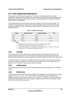
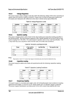
Design and Environmental Specifications Intel® Server Board S3420GP TPS Note: 1. The 5 VSB output voltage rise time should be from 1.0 ms to 25.0 ms. Item Tsb_on_delay Tac_on_delay Tvout_holdup Tpwok_holdup Tpson_on_delay Tpson_pwok Tpwok_on Tpwok_off Tpwok_low Tsb_vout Figure 41. Output Voltage Timing Table 70. Turn On/Off Timing Description Delay from AC being applied to 5 VSB being within regulation. Delay from AC being applied to all output voltages being within regulation. Duration for which all output voltages stay within regulation after loss of AC. Measured at 80% of maximum load. Delay from loss of AC to de-assertion of PWOK. Measured at 80% of maximum load. Delay from PSON# active to output voltages within regulation limits. Delay from PSON# deactive to PWOK being deasserted. Delay from output voltages within regulation limits to PWOK asserted at turn on. Delay from PWOK de-asserted to output voltages (3.3 V, 5 V, 12 V, -12 V) dropping out of regulation limits. Duration of PWOK being in the de-asserted state during an off/on cycle using AC or the PSON signal. Delay from 5 VSB being in regulation to O/Ps being in regulation at AC turn on. Minimum N/A N/A 21 20 5 N/A 100 1 100 50 Maximum 1500 2500 N/A N/A 400 50 500 N/A N/A 1000 Units Msec Msec Msec Msec Msec Msec Msec Msec Msec Msec 102 Revision 2.4 Intel order number E65697-010
-
 1
1 -
2
-
3
-
4
-
5
-
6
-
7
-
8
-
9
-
10
-
11
-
12
-
13
-
14
-
15
-
16
-
17
-
18
-
19
-
20
-
21
-
22
-
23
-
24
-
25
-
26
-
27
-
28
-
29
-
30
-
31
-
32
-
33
-
34
-
35
-
36
-
37
-
38
-
39
-
40
-
41
-
42
-
43
-
44
-
45
-
46
-
47
-
48
-
49
-
50
-
51
-
52
-
53
-
54
-
55
-
56
-
57
-
58
-
59
-
60
-
61
-
62
-
63
-
64
-
65
-
66
-
67
-
68
-
69
-
70
-
71
-
72
-
73
-
74
-
75
-
76
-
77
-
78
-
79
-
80
-
81
-
82
-
83
-
84
-
85
-
86
-
87
-
88
-
89
-
90
-
91
-
92
-
93
-
94
-
95
-
96
-
97
-
98
-
99
-
100
-
101
-
102
-
103
-
104
-
105
-
106
-
107
-
108
-
 109
109 -
 110
110 -
 111
111 -
 112
112 -
 113
113 -
 114
114 -
 115
115 -
 116
116 -
 117
117 -
 118
118 -
 119
119 -
120
-
121
-
122
-
123
-
124
-
125
-
126
-
127
-
128
-
129
-
130
-
131
-
132
-
133
-
134
-
135
-
136
-
137
-
138
-
139
-
140
-
141
-
142
-
143
-
144
 |
 |
