Intel S3420GPLC Product Specification - Page 94
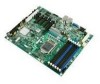
Rear NIC and USB connector
 |
UPC - 735858211819
View all Intel S3420GPLC manuals
Add to My Manuals
Save this manual to your list of manuals |
Page 94 highlights
Connector/Header Locations and Pin-outs Intel® Server Board S3420GP TPS Pin Signal Name 3 V_IO_B_CONN 4 TP_VID_CONN_B4 5 GND 6 GND 7 GND 8 GND 9 TP_VID_CONN_B9 10 GND 11 TP_VID_CONN_B11 12 V_IO_DDCDAT 13 V_IO_HSYNC_CONN 14 V_IO_VSYNC_CONN 15 V_IO_DDCCLK Description Blue (analog color signal B) No connection Ground Ground Ground Ground No connection Ground No connection DDCDAT HSYNC (horizontal sync) VSYNC (vertical sync) DDCCLK 7.5.2 Rear NIC and USB connector The server board provides two stacked RJ-45/2xUSB connectors side-by-side on the back edge of the board (J6A1, J5A1). The pin-out for NIC connectors are identical and defined in the following table. Table 48. RJ-45 10/100/1000 NIC Connector Pin-out (J5A1) Pin 1 3 5 7 9 11 13 15 17 19 21 Signal Name P5V_USB_PWR75 USB_PCH_11_FB_DP P5V_USB_PWR75 USB_PCH_10_FB_DP P1V9_LAN2_R NIC2_MDIN NIC2_MDIN NIC2_MDIN NIC2_MDIN LED_NIC2_1 LED_NIC2_LINK100_R_0 Pin Signal Name 2 USB_PCH_11_FB_DN 4 GND 6 USB_PCH_10_FB_DN 8 GND 10 NIC2_MDIP 12 NIC2_MDIP 14 NIC2_MDIP 16 NIC2_MDIP 18 GND 20 P3V3_AUX 22 LED_NIC2_LINK1000_2 Pin 1 3 5 7 9 11 13 15 17 19 Table 49. RJ-45 10/100/1000 NIC Connector Pin-out (J6A1) Signal Name P5V_USB_PWR75 USB_PCH_11_FB_DP P5V_USB_PWR75 USB_PCH_10_FB_DP P1V8_PHY_VCT_R NIC1_MDIN NIC1_MDIN NIC1_MDIN NIC1_MDIN LED_NIC1_LINK_ACT_0_R Pin 2 4 6 8 10 12 14 16 18 20 Signal Name USB_PCH_11_FB_DN GND USB_PCH_10_FB_DN GND NIC1_MDIP NIC1_MDIP NIC2_MDIP NIC2_MDIP GND P3V3_AUX 82 Intel order number E65697-010 Revision 2.4
-
 1
1 -
2
-
3
-
4
-
5
-
6
-
7
-
8
-
9
-
10
-
11
-
12
-
13
-
14
-
15
-
16
-
17
-
18
-
19
-
20
-
21
-
22
-
23
-
24
-
25
-
26
-
27
-
28
-
29
-
30
-
31
-
32
-
33
-
34
-
35
-
36
-
37
-
38
-
39
-
40
-
41
-
42
-
43
-
44
-
45
-
46
-
47
-
48
-
49
-
50
-
51
-
52
-
53
-
54
-
55
-
56
-
57
-
58
-
59
-
60
-
61
-
62
-
63
-
64
-
65
-
66
-
67
-
68
-
69
-
70
-
71
-
72
-
73
-
74
-
75
-
76
-
77
-
78
-
79
-
80
-
81
-
82
-
83
-
84
-
85
-
86
-
87
-
88
-
 89
89 -
 90
90 -
 91
91 -
 92
92 -
 93
93 -
 94
94 -
 95
95 -
 96
96 -
 97
97 -
 98
98 -
 99
99 -
100
-
101
-
102
-
103
-
104
-
105
-
106
-
107
-
108
-
109
-
110
-
111
-
112
-
113
-
114
-
115
-
116
-
117
-
118
-
119
-
120
-
121
-
122
-
123
-
124
-
125
-
126
-
127
-
128
-
129
-
130
-
131
-
132
-
133
-
134
-
135
-
136
-
137
-
138
-
139
-
140
-
141
-
142
-
143
-
144
 |
 |
