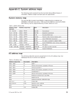
Lenovo NetVista A22 User guide for NetVista 2254, 2256, 2257, 6336, 6337, 6339 - Page 75
Appendix C. System address maps, System memory map, I/O address map
 |
View all Lenovo NetVista A22 manuals
Add to My Manuals
Save this manual to your list of manuals |
Page 75 highlights
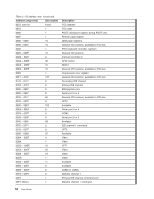
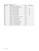
Appendix C. System address maps The following charts represent how the hard disk stores different types of information. Address ranges and byte sizes are approximate. System memory map The first 640 KB of system board RAM is mapped starting at address hex 00000000. A 256-byte area and a 1 KB area of this RAM are reserved for BIOS data. Memory can be mapped differently if POST detects an error. Table 1. System memory map Address range (decimal) Address range (hex) 0 K - 512 KB 00000 - 7FFFF 512 K - 639 KB 80000 - 9FBFF 639 K - 640 KB 9FC00 - 9FFFF 640 K - 767 KB A0000 - BFFFF 768 K - 800 KB C0000 - C7FFF 800 K - 896 KB C8000 - DFFFF 896 K - 1 MB E0000 - FFFFF 1 MB - 16 MB 1000000 - FFFFFF 16 MB - 4096 MB 10000000 - FFDFFFFF FFFE0000 - FFFFFFFF Size 512 KB 127 KB 1 KB 128 KB 32 KB 96 KB 128 KB 15 MB 4080 MB 128 KB Description Conventional Extended conventional Extended BIOS data Dynamic video memory display cache Video ROM BIOS (shadowed) PCI space, available to adapter ROMs System ROM BIOS (main memory shadowed) PCI space PCI space (positive decode) System ROM BIOS I/O address map The following table lists resource assignments for the I/O address map. Any addresses that are not shown are reserved. Table 2. I/O address map Address range (hex) 0000 - 000F 0010 - 001F 0020 - 0021 0022 - 003F 0040 - 0043 0044 - 00FF 0060 0061 0064 0070, bit 7 0070, bits 6:0 0071 0072 Size (bytes) 16 16 2 30 4 28 1 1 1 1 bit 6 bits 1 1 bit Description DMA 1 General I/O locations, available to PCI bus Interrupt controller 1 General I/O locations, available to PCI bus Counter/timer 1 General I/O locations, available to PCI bus Keyboard controller byte, reset IRQ System port B Keyboard controller, CMD/ATAT byte Enable NMI Real-time clock, address Real-time clock, data Enable NMI © Copyright IBM Corp. 2001 63
-
 1
1 -
2
-
3
-
4
-
5
-
6
-
7
-
8
-
9
-
10
-
11
-
12
-
13
-
14
-
15
-
16
-
17
-
18
-
19
-
20
-
21
-
22
-
23
-
24
-
25
-
26
-
27
-
28
-
29
-
30
-
31
-
32
-
33
-
34
-
35
-
36
-
37
-
38
-
39
-
40
-
41
-
42
-
43
-
44
-
45
-
46
-
47
-
48
-
49
-
50
-
51
-
52
-
53
-
54
-
55
-
56
-
57
-
58
-
59
-
60
-
61
-
62
-
63
-
64
-
65
-
66
-
67
-
68
-
69
-
 70
70 -
 71
71 -
 72
72 -
 73
73 -
 74
74 -
 75
75 -
 76
76 -
 77
77 -
 78
78 -
 79
79 -
 80
80 -
81
-
82
-
83
-
84
-
85
-
86
 |
 |