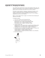
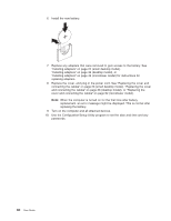
Lenovo NetVista A22 User guide for NetVista 2254, 2256, 2257, 6336, 6337, 6339 - Page 76
Address range hex, Size bytes, Description, General I/O locations
 |
View all Lenovo NetVista A22 manuals
Add to My Manuals
Save this manual to your list of manuals |
Page 76 highlights
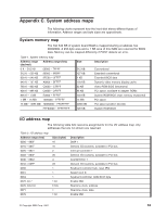
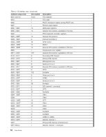
Table 2. I/O address map (continued) Address range (hex) Size (bytes) 0072, bits 6:0 6 bits 0073 1 0080 1 008F 1 0080 - 008F 16 0090 - 0091 15 0092 1 0093 - 009F 15 00A0 - 00A1 2 00A2 - 00BF 30 00C0 - 00DF 31 00E0 - 00EF 16 00F0 1 00F1 - 016F 127 0170 - 0177 8 01F0 - 01F7 8 0200 - 0207 8 0220 - 0227 8 0228 - 0277 80 0278 - 027F 8 0280 - 02E7 102 02E8 - 02EF 8 02F8 - 02FF 8 0338 - 033F 8 0340 - 036F 48 0370 - 0371 2 0378 - 037F 8 0380 - 03B3 52 03B4 - 03B7 4 03BA 1 03BC - 03BE 16 03C0 - 03CF 52 03D4 - 03D7 16 03DA 1 03D0 - 03DF 11 03E0 - 03E7 8 03E8 - 03EF 8 03F0 - 03F5 6 03F6 1 03F7 (Write) 1 Description RTC address RTC data POST checkpoint register during POST only Refresh page register DMA page registers General I/O locations, available to PCI bus PS/2 keyboard controller registers General I/O locations Interrupt controller 2 APM control DMA 2 General I/O locations, available to PCI bus Coprocessor error register General I/O locations, available to PCI bus Secondary IDE channel Primary IDE channel MIDI/joystick port Serial port 3 or 4 General I/O locations, available to PCI bus LPT3 Available Serial port 3 or 4 COM2 Serial port 3 or 4 Available IDE channel 1 command LPT2 Available Video Video LPT1 Video Video Video Available Available COM3 or COM4 Diskette channel 1 Primary IDE channel command port Diskette channel 1 command 64 User Guide
-
 1
1 -
2
-
3
-
4
-
5
-
6
-
7
-
8
-
9
-
10
-
11
-
12
-
13
-
14
-
15
-
16
-
17
-
18
-
19
-
20
-
21
-
22
-
23
-
24
-
25
-
26
-
27
-
28
-
29
-
30
-
31
-
32
-
33
-
34
-
35
-
36
-
37
-
38
-
39
-
40
-
41
-
42
-
43
-
44
-
45
-
46
-
47
-
48
-
49
-
50
-
51
-
52
-
53
-
54
-
55
-
56
-
57
-
58
-
59
-
60
-
61
-
62
-
63
-
64
-
65
-
66
-
67
-
68
-
69
-
70
-
 71
71 -
 72
72 -
 73
73 -
 74
74 -
 75
75 -
 76
76 -
 77
77 -
 78
78 -
 79
79 -
 80
80 -
 81
81 -
82
-
83
-
84
-
85
-
86
 |
 |