Intel SE7505VB2 Product Specification - Page 22
MCH Memory Architecture Overview, ICH4: I/O Controller Hub 4. - server
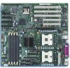 |
View all Intel SE7505VB2 manuals
Add to My Manuals
Save this manual to your list of manuals |
Page 22 highlights
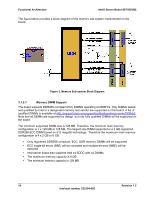
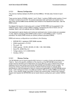
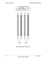
Functional Architecture Intel® Server Board SE7505VB2 ICH4: I/O Controller Hub 4. The ICH4 controller has several components. It provides the interface for a 32-bit/33-MHz PCI bus. The ICH4 can be both a master and a target on that PCI bus. The ICH4 also includes a USB 2.0 controller and an IDE controller. The ICH4 is also responsible for much of the power management functions, with ACPI control registers built in. The ICH4 also provides a number of GPIO pins and has the LPC bus to support low speed legacy I/O. The MCH, P64H2, and ICH4 chips provide the pathway between processor and I/O systems. The MCH is responsible for accepting access requests from the host (processor) bus, and directing all I/O accesses to one of the PCI buses or legacy I/O locations. If the cycle is directed to one of the 64-bit PCI segments, the MCH communicates with the P64H2 through a private interface called the HI (Hub Interface). If the cycle is directed to the ICH4, the cycle is output on the MCH's 8-bit HI 1.5 bus. The P64H2 translates the HI 2.0 bus operation to a 64-bit PCI signaling environment operating between 133 MHz and 33 MHz. The HI 2.0 bus is 16 bits wide and operates at 66 MHz with 512MT/s, providing over 1 GB per second of bandwidth. All I/O for the board, including PCI and PC-compatible I/O, is directed through the MCH and then through either the P64H2 or the ICH4 provided PCI buses. The ICH4 provides one 32-bit/33-MHz PCI bus hereafter called P32-A. The P64H2 provides one 64-bit/100-MHz PCI-X bus, hereafter called P64-B, and one 64bit/66MHz PCI bus, hereafter called P64-C. This independent bus structure allows all three PCI buses to operate independently and concurrently providing additional bandwidth to the system. 3.2.1 MCH Memory Architecture Overview The MCH supports a 144-bit wide memory sub-system that can support a maximum of 8 GB of DDR266 memory using 2 GB DIMMs. This configuration needs external registers for buffering the memory address and control signals. The four chip selects are registered inside the MCH and need no external registers for chip selects. The memory interface runs at 266MT/s. The memory interface supports a 72-bit or 144-bit wide memory array. It uses fifteen address lines (BA [1:0] and MA [12:0]) and supports 64 Mb, 128 Mb, 256 Mb, 512 Mb DRAM densities. The DDR DIMM interface supports memory scrubbing, single-bit error correction, and multiple bit error detection and Intel x4 SDDC with x4 DIMMs. 22 Revision 1.2 Intel part number C32194-002
-
 1
1 -
2
-
3
-
4
-
5
-
6
-
7
-
8
-
9
-
10
-
11
-
12
-
13
-
14
-
15
-
16
-
 17
17 -
 18
18 -
 19
19 -
 20
20 -
 21
21 -
 22
22 -
 23
23 -
 24
24 -
 25
25 -
 26
26 -
 27
27 -
28
-
29
-
30
-
31
-
32
-
33
-
34
-
35
-
36
-
37
-
38
-
39
-
40
-
41
-
42
-
43
-
44
-
45
-
46
-
47
-
48
-
49
-
50
-
51
-
52
-
53
-
54
-
55
-
56
-
57
-
58
-
59
-
60
-
61
-
62
-
63
-
64
-
65
-
66
-
67
-
68
-
69
-
70
-
71
-
72
-
73
-
74
-
75
-
76
-
77
-
78
-
79
-
80
-
81
-
82
-
83
-
84
-
85
-
86
-
87
-
88
-
89
-
90
-
91
-
92
-
93
-
94
-
95
-
96
-
97
-
98
-
99
-
100
-
101
-
102
-
103
-
104
-
105
-
106
-
107
-
108
 |
 |