Intel SE7505VB2 Product Specification - Page 66
Configuration Jumpers, System Recovery and Update Jumpers - bios update
 |
View all Intel SE7505VB2 manuals
Add to My Manuals
Save this manual to your list of manuals |
Page 66 highlights
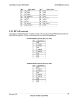
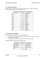
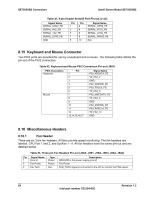
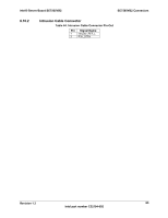
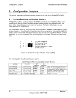
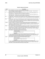
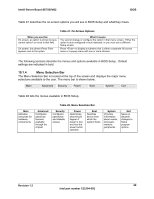
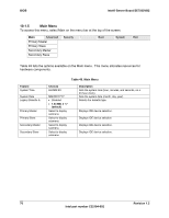
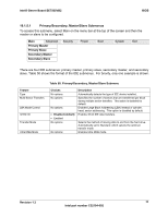
Configuration Jumpers Intel® Server Board SE7505VB2 9. Configuration Jumpers This section describes configuration jumper options on the Intel Server Board SE7505VB2. 9.1 System Recovery and Update Jumpers A 10-pin block (J4J1), located just below the DIMM connectors, provides a total of four 2-pin jumper blocks that are used to configure several system recovery and update options. The figure below shows the jumper pins and their functions. The factory defaults are set to a protected mode for each function. Two jumpers are stored on four pins during normal operation. The BIOS bootblock write protect jumper on pins 7-8 should be left on these pins at all times except when instructed by the BIOS release notes to remove it. The jumper stored on pins 9-10 is used to perform different functions depending on the pins it is placed. For normal operation, this jumper should be on the storage pins. 2 10 1-2 Clear Password 3-4 Recovery Mode 5-6 Clear CMOS 7-8 BIOS Boot Block Protect 1 9 9-10 Reserved Figure 10. System Recovery and Update Jumpers (J4J1) The following table describes each jumper option. Table 45. System Recovery and Update Jumper Options Function Clear Password Pin - Pin 1 - 2 (J4J1 pin 1-2) Off (open=1) Disable Recovery Mode 3 - 4 (J4J1 pin 3-4) Disable Clear CMOS 5 - 6 (J4J1 Pin 5-6) Disable BIOS boot block protect 7 - 8 (J4J1 pin 7-8) Disable Storage location 9 - 10 (J4J1 pin 9-10) N/A On (close=0) Enable Enable Enable Enable N/A Description These four pins are connected to GPIs of SIO. The system BIOS reads these GPIs status and decides whether or not to execute related task. The clear CMOS status is reflected to ICH4. Defaults are in bold. 66 Revision 1.2 Intel part number C32194-002
-
 1
1 -
2
-
3
-
4
-
5
-
6
-
7
-
8
-
9
-
10
-
11
-
12
-
13
-
14
-
15
-
16
-
17
-
18
-
19
-
20
-
21
-
22
-
23
-
24
-
25
-
26
-
27
-
28
-
29
-
30
-
31
-
32
-
33
-
34
-
35
-
36
-
37
-
38
-
39
-
40
-
41
-
42
-
43
-
44
-
45
-
46
-
47
-
48
-
49
-
50
-
51
-
52
-
53
-
54
-
55
-
56
-
57
-
58
-
59
-
60
-
 61
61 -
 62
62 -
 63
63 -
 64
64 -
 65
65 -
 66
66 -
 67
67 -
 68
68 -
 69
69 -
 70
70 -
 71
71 -
72
-
73
-
74
-
75
-
76
-
77
-
78
-
79
-
80
-
81
-
82
-
83
-
84
-
85
-
86
-
87
-
88
-
89
-
90
-
91
-
92
-
93
-
94
-
95
-
96
-
97
-
98
-
99
-
100
-
101
-
102
-
103
-
104
-
105
-
106
-
107
-
108
 |
 |