Asus P I-P55SP3AV P/I-P55SP3AV User's manual - Page 39
Asus P I-P55SP3AV Manual
 |
View all Asus P I-P55SP3AV manuals
Add to My Manuals
Save this manual to your list of manuals |
Page 39 highlights
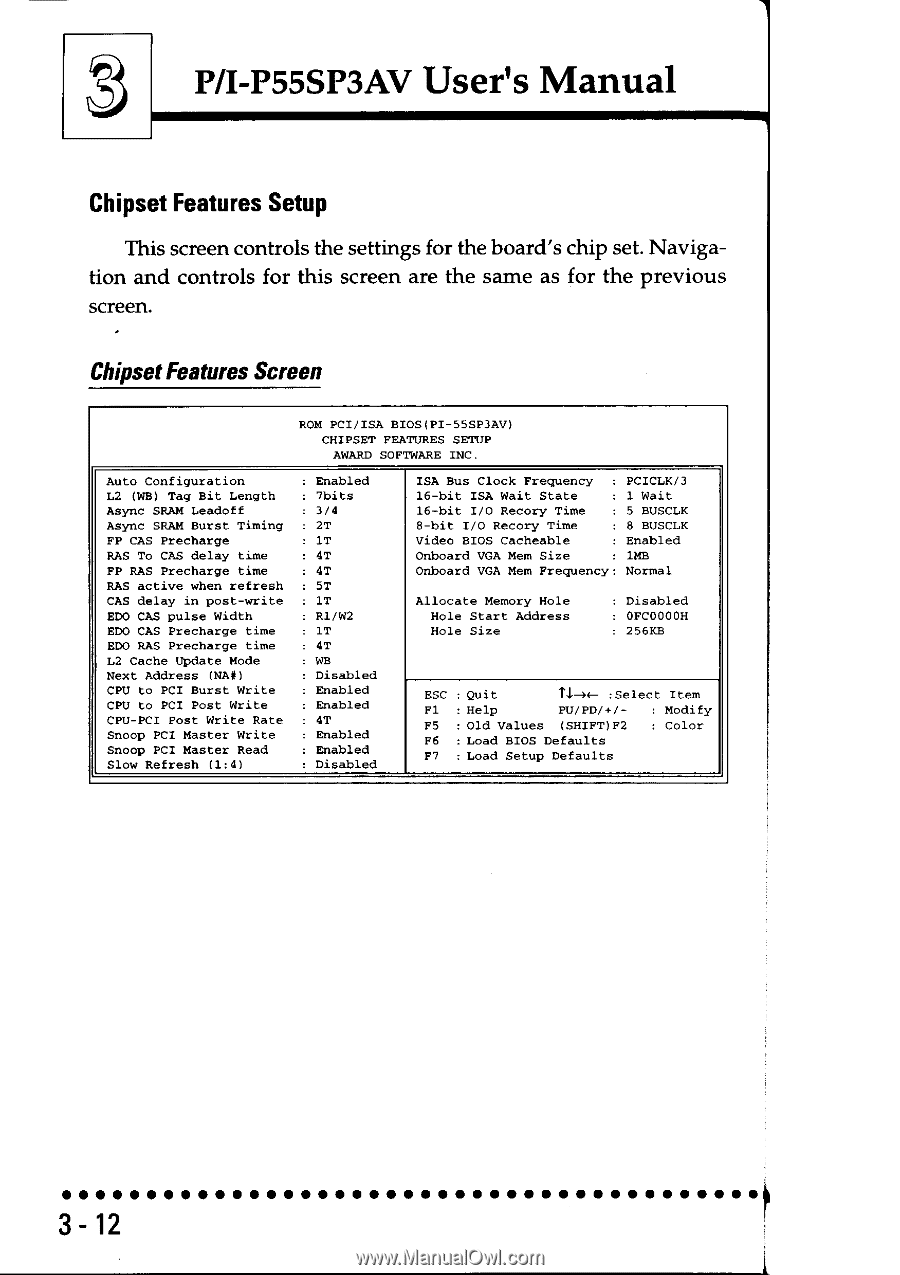
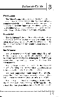
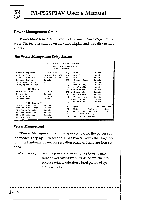
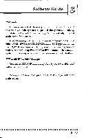
1 P/I-P55SP3AV User's Manual Chipset Features Setup This screen controls the settings for the board's chip set. Navigation and controls for this screen are the same as for the previous screen. ChipsetFeatures Screen ROM PCI/ISA BIOS(PI-55SP3AV) CHIPSET FEATURES SETUP AWARD SOFTWARE INC. Auto Configuration L2 (WB) Tag Bit Length Async SRAM Leadoff Async SRAM Burst Timing FP CAS Precharge RAS To CAS delay time FP RAS Precharge time RAS active when refresh CAS delay in post-write EDO CAS pulse Width EDO CAS Precharge time EDO RAS Precharge time L2 Cache Update Mode Next Address (NAM) CPU to PCI Burst Write CPU to PCI Post Write CPU-PCI Post Write Rate Snoop PCI Master Write Snoop PCI Master Read Slow Refresh (1:4) : Enabled : 7bits : 3/4 : 2T : 1T : 4T : 4T : 5T : 1T : R1/W2 : 1T : 4T : WB : Disabled : Enabled : Enabled : 4T : Enabled : Enabled : Disabled ISA Bus Clock Frequency : PCICLK/3 16-bit ISA Wait State : 1 Wait 16-bit I/O Recory Time : 5 BUSCLK 8-bit I/O Recory Time : 8 BUSCLK Video BIOS Cacheable : Enabled Onboard VGA Mem Size : 1MB Onboard VGA Mem Frequency: Normal Allocate Memory Hole Hole Start Address Hole Size : Disabled : OFC0000H : 256KB ESC : Quit Ti-n- :Select Item Fl : Help PU/PD/+/- Modify F5 : Old Values (SHIFT)F2 Color F6 : Load BIOS Defaults F7 : Load Setup Defaults OOOOOOO 3-12 OOOOOOOOOOOOOOOOOOOO
-
 1
1 -
2
-
3
-
4
-
5
-
6
-
7
-
8
-
9
-
10
-
11
-
12
-
13
-
14
-
15
-
16
-
17
-
18
-
19
-
20
-
21
-
22
-
23
-
24
-
25
-
26
-
27
-
28
-
29
-
30
-
31
-
32
-
33
-
 34
34 -
 35
35 -
 36
36 -
 37
37 -
 38
38 -
 39
39 -
 40
40 -
 41
41 -
 42
42 -
 43
43 -
 44
44 -
45
-
46
-
47
-
48
-
49
-
50
-
51
-
52
-
53
-
54
-
55
-
56
-
57
-
58
-
59
-
60
-
61
-
62
-
63
-
64
-
65
-
66
-
67
-
68
-
69
-
70
-
71
-
72
-
73
-
74
-
75
-
76
-
77
-
78
-
79
-
80
-
81
-
82
 |
 |