Foxconn MARS English Manual. - Page 48
► Write to Read Delay tWTR
 |
View all Foxconn MARS manuals
Add to My Manuals
Save this manual to your list of manuals |
Page 48 highlights
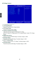
3 ► DRAM Timing Selectable This item is used to enable/disable provision of DRAM timing by SPD device. The Serial Presence Detect (SPD) device is a small EEPROM chip, mounted on a DDR2 memory module. It contains important information about the module's speed, size, addressing mode and various other parameters, so that the motherboard memory controller (chipset) can better access the memory. ► CAS Latency Time (tCL) This item controls the CAS latency, which determines the timing delay (in clock cycles) before SDRAM starts a read command after receiving it. ► RAS# to CAS# Delay (tRCD) This item allows you to select a delay time (in clock cycles) between the CAS and RAS strobe signals. ► RAS# Precharge (tRP) This item allows you to select the DRAM RAS precharge time (in clock cycles). ► Precharge Delay (tRAS) This item allows you to set the precharge delay time (in clock cycles). ► Write to Precharge (tWR) This item allows you to set Write to Precharge delay (in clock cycles). ► Row Refresh Cycle (tRFC) This item allows you to set Row Refresh Cycle (in clock cycles). ► Write to Read Delay (tWTR) This item allows you to set minimum Write-to-read delay (in clock cycles). ► Row to Row Delay (tRRD) This item allows you to set Row to Row Delay (in clock cycles). ► Read to Precharge (tRPT) This item is used to set the read CAS to precharge time (in clock cycles). ► Fast Chip Select This item used to enable or disable the fast chip select signal of the DDR RAM. ► Clock Per Command This item is used to set the Clock Per Command for your memory. (in clock cycles). ► Memory Channel0 DLL Adjust The DLL stand for Delay Lock Loop, and it uses a symmetrical delay line for tight locking on both the rising and falling edges of DRAM. This is to adjust Channel 0 DDR2 timing. ► Memory Channel1 DLL Adjust This is to adjust Channel 1 DDR2 timing. ► Refresh Count Adjust In merged DRAM circuit, the DRAM could suffer from shorter data retention time because of heat and noise caused by the logic portion. Frequent refreshes increase power consumption. Also, they disturb normal DRAM accesses leading to performance degradation. In order to overcome this problem, we propose several DRAM refresh architectures. ► Performance Level User can run freeware program such as Memset to find out the performance level of your motherboard. For example, if the performance level tested and read is 5, then user can set this level setting to 4 to over drive the memory or set the level to 6 to slow down the memory access. Lower value in this setting means faster speed. 41
-
 1
1 -
2
-
3
-
4
-
5
-
6
-
7
-
8
-
9
-
10
-
11
-
12
-
13
-
14
-
15
-
16
-
17
-
18
-
19
-
20
-
21
-
22
-
23
-
24
-
25
-
26
-
27
-
28
-
29
-
30
-
31
-
32
-
33
-
34
-
35
-
36
-
37
-
38
-
39
-
40
-
41
-
42
-
 43
43 -
 44
44 -
 45
45 -
 46
46 -
 47
47 -
 48
48 -
 49
49 -
 50
50 -
 51
51 -
 52
52 -
 53
53 -
54
-
55
-
56
-
57
-
58
-
59
-
60
-
61
-
62
-
63
-
64
-
65
-
66
-
67
-
68
-
69
-
70
-
71
-
72
-
73
-
74
-
75
-
76
-
77
-
78
-
79
-
80
-
81
-
82
-
83
-
84
-
85
-
86
-
87
-
88
-
89
-
90
-
91
-
92
-
93
-
94
-
95
-
96
-
97
-
98
-
99
-
100
-
101
-
102
-
103
-
104
-
105
-
106
-
107
-
108
-
109
-
110
 |
 |
