Intel SE7505VB2 Product Specification - Page 16
Functional Architecture, Processor and Memory Subsystem, Processor Support - memory support
 |
View all Intel SE7505VB2 manuals
Add to My Manuals
Save this manual to your list of manuals |
Page 16 highlights
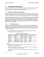
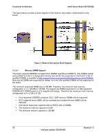
Functional Architecture Intel® Server Board SE7505VB2 3. Functional Architecture This chapter provides a high-level description of the functionality distributed between the architectural blocks of the Intel® Server Board SE7505VB2. 3.1 Processor and Memory Subsystem The Intel® chipset E7505 provides a 36-bit address, 64-bit data processor host bus interface, operating at 533 MHz in the AGTL+ signaling environment. The MCH component of the chipset provides an integrated memory controller, an 8-bit hub interface, and one 16-bit hub interfaces. The hub interface provides the interface to two 64-bit/100-MHz PCI-X buses and one 64-bit/66MHz PCI bus via the P64H2, and the interface to two 32-bit/33-MHz PCI buses via the ICH4. The board directly supports up to 8 GB of ECC memory, using four DDR266 compliant ECC DIMMs. The ECC implementation in the MCH can detect and correct single-bit errors (SBE), detect multiple-bit errors (MBE), and supports Intel® x4 Single Data Device Correction (Intel x4 SDDC) feature with x4 DIMMs. 3.1.1 Processor Support The Intel Server Board SE7505VB2 supports one or two processors in the 604-pin FCPGA package. When two processors are installed, all processors must be of identical revision, core voltage, and bus/core speed. When only one processor is installed, it should be in the socket labeled CPU1 and the other socket must be empty. The support circuitry on the server board consists of the following: Dual 604-pin processor sockets supporting 533MHz FSB Intel Xeon processors. Processor host bus AGTL+ support circuitry. Table 1. Processor Support Matrix Processor Family Package Type Intel Xeon FCPGA Intel Xeon FCPGA Intel Xeon FCPGA Intel Xeon mPGA / FCPGA Intel Xeon mPGA / FCPGA Intel Xeon mPGA / FCPGA Intel Xeon mPGA / FCPGA Frequency 3.06GHz 2.8 GHz 2.67 GHz 2.4 GHz 2.2 GHz 2.0GHz 1.8GHz Cache Size 512KB 512KB 512KB 512KB 512KB 512KB 512KB Front Side Bus Speed 533 400 / 533 400 / 533 400 / 533 400 / 533 400 / 533 400 Notes: Processors must be populated in sequential order. Processor socket 1 must be populated before processor socket 2. The board is designed to provide up to 65A of current per processor. Processors with higher current requirements are not supported. No terminator is required in the second processor socket when using a uni-processor configuration. 16 Revision 1.2 Intel part number C32194-002
-
 1
1 -
2
-
3
-
4
-
5
-
6
-
7
-
8
-
9
-
10
-
 11
11 -
 12
12 -
 13
13 -
 14
14 -
 15
15 -
 16
16 -
 17
17 -
 18
18 -
 19
19 -
 20
20 -
 21
21 -
22
-
23
-
24
-
25
-
26
-
27
-
28
-
29
-
30
-
31
-
32
-
33
-
34
-
35
-
36
-
37
-
38
-
39
-
40
-
41
-
42
-
43
-
44
-
45
-
46
-
47
-
48
-
49
-
50
-
51
-
52
-
53
-
54
-
55
-
56
-
57
-
58
-
59
-
60
-
61
-
62
-
63
-
64
-
65
-
66
-
67
-
68
-
69
-
70
-
71
-
72
-
73
-
74
-
75
-
76
-
77
-
78
-
79
-
80
-
81
-
82
-
83
-
84
-
85
-
86
-
87
-
88
-
89
-
90
-
91
-
92
-
93
-
94
-
95
-
96
-
97
-
98
-
99
-
100
-
101
-
102
-
103
-
104
-
105
-
106
-
107
-
108
 |
 |