Intel SE7505VB2 Product Specification - Page 31
Clock Generation and Distribution, MHz at 3.3V logic levels: For ICH4, PCI Connector, sIO and FWH - server board driver
 |
View all Intel SE7505VB2 manuals
Add to My Manuals
Save this manual to your list of manuals |
Page 31 highlights
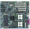
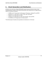
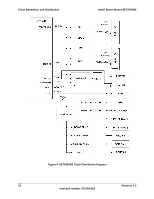
Intel® Server Board SE7505VB2 Clock Generation and Distribution 4. Clock Generation and Distribution All buses on the Intel Server Board SE7505VB2 operate using synchronous clocks. Clock synthesizer/driver circuitry on the baseboard generates clock frequencies and voltage levels as required, including the following: 100 MHz at 3.3 V logic levels. For Processor 0, Processor 1, Debug Port and MCH. 66 MHz at 3.3 V logic levels: For MCH, ICH4, AGP, and P64H2 48 MHz at 3.3V logic levels: For ICH4 33 MHz at 3.3V logic levels: For ICH4, PCI Connector, sIO and FWH 14.318 MHz at 2.5 V logic levels: For ICH4 and sIO The following figure illustrates clock generation and distribution on the board. Revision 1.2 31 Intel part number C32194-002
-
 1
1 -
2
-
3
-
4
-
5
-
6
-
7
-
8
-
9
-
10
-
11
-
12
-
13
-
14
-
15
-
16
-
17
-
18
-
19
-
20
-
21
-
22
-
23
-
24
-
25
-
 26
26 -
 27
27 -
 28
28 -
 29
29 -
 30
30 -
 31
31 -
 32
32 -
 33
33 -
 34
34 -
 35
35 -
 36
36 -
37
-
38
-
39
-
40
-
41
-
42
-
43
-
44
-
45
-
46
-
47
-
48
-
49
-
50
-
51
-
52
-
53
-
54
-
55
-
56
-
57
-
58
-
59
-
60
-
61
-
62
-
63
-
64
-
65
-
66
-
67
-
68
-
69
-
70
-
71
-
72
-
73
-
74
-
75
-
76
-
77
-
78
-
79
-
80
-
81
-
82
-
83
-
84
-
85
-
86
-
87
-
88
-
89
-
90
-
91
-
92
-
93
-
94
-
95
-
96
-
97
-
98
-
99
-
100
-
101
-
102
-
103
-
104
-
105
-
106
-
107
-
108
 |
 |

Intel® Server Board SE7505VB2
Clock Generation and Distribution
4.
Clock Generation and Distribution
All buses on the Intel Server Board SE7505VB2 operate using synchronous clocks.
Clock
synthesizer/driver circuitry on the baseboard generates clock frequencies and voltage levels as
required, including the following:
±
100 MHz at 3.3 V logic levels. For Processor 0, Processor 1, Debug Port and MCH.
±
66 MHz at 3.3 V logic levels: For MCH, ICH4, AGP, and P64H2
±
48 MHz at 3.3V logic levels: For ICH4
±
33 MHz at 3.3V logic levels: For ICH4, PCI Connector, sIO and FWH
±
14.318 MHz at 2.5 V logic levels: For ICH4 and sIO
The following figure illustrates clock generation and distribution on the board.
Revision 1.2
Intel part number C32194-002
31