Intel SE7505VB2 Product Specification - Page 21
I2C Bus, DRAM ECC, The Intel® E7505 Chipset, Intel® Server Board SE7505VB2, Functional Architecture
 |
View all Intel SE7505VB2 manuals
Add to My Manuals
Save this manual to your list of manuals |
Page 21 highlights
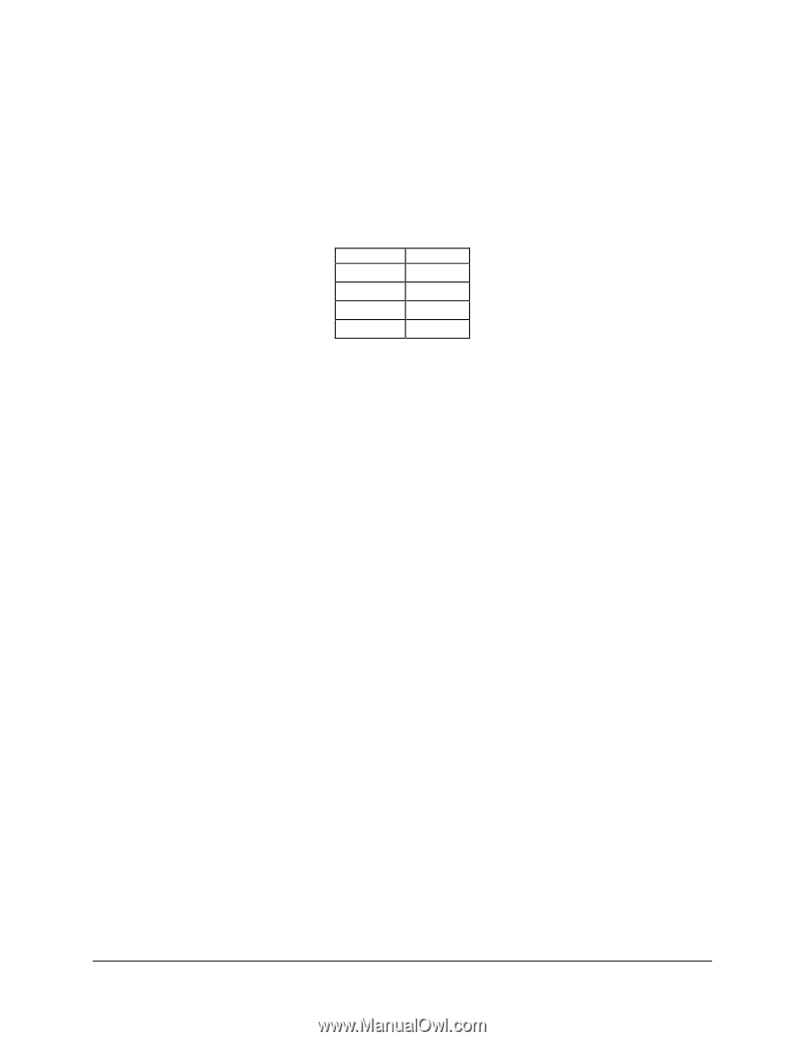
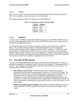
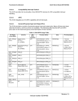
Intel® Server Board SE7505VB2 Functional Architecture 3.1.2.4 I2C Bus The I2C bus is used by the system BIOS to retrieve DIMM information needed to program the MCH memory registers, which are required to boot the system. The following table provides the I2C addresses for each DIMM slot. Table 3. I2C Addresses for Memory Module SMB Device DIMM 1A DIMM 1B DIMM 2A DIMM 2B Address 0xA0 0xA2 0xA4 0xA6 3.1.2.5 DRAM ECC The ECC used for DRAM provides Intel x4 SDDC technology for x4 SDRAMs. DRAMs that are x8 use the same algorithm but will not have Intel x4 SDDC technology, since at most only four bits can be corrected with this ECC. The method provides more ECC bits so each ECC word can correct more than a single-bit failure. This is possible because different mathematical algorithms provide multiple-bit correction with the right number of data bits and ECC bits. For example, a 144-bit ECC word that consists of 128 data bits and 16 ECC bits can be used to correct up to 4 bit errors within certain bit fields of data. These four bits must be adjacent, not random. Even though the ratio of the ECC bits to data bits is the same as the previous example (16/128 vs. 8/64), the longer ECC word allows for a correction and detection algorithm that is more efficient. 3.2 The Intel® E7505 Chipset The Intel Server Board SE7505VB2 is designed around the Intel E7505 chipset. The chipset provides an integrated I/O bridge and memory controller, and a flexible I/O subsystem core (PCI / PCI-X) . This is targeted for multiprocessor systems and standard high-volume servers. The chipset consists of three components: MCH: Memory Control Hub. The MCH accepts access requests from the host (processor) bus and directs those accesses to memory or to one of the PCI buses. The MCH monitors the host bus, examining addresses for each request. Accesses may be directed to a memory request queue for subsequent forwarding to the memory subsystem, or to an outbound request queue for subsequent forwarding to one of the PCI buses. The MCH also accepts inbound requests from the P64H2 and the ICH4. The MCH is responsible for generating the appropriate controls to control data transfer to and from memory. P64H2: PCI-X 64bit Hub 2.0 I/O Bridge. The P64H2 provides the interface for two PCIX buses capable of 133MHz operation. The P64H2 is both master and target on both buses. Revision 1.2 21 Intel part number C32194-002
-
 1
1 -
2
-
3
-
4
-
5
-
6
-
7
-
8
-
9
-
10
-
11
-
12
-
13
-
14
-
15
-
 16
16 -
 17
17 -
 18
18 -
 19
19 -
 20
20 -
 21
21 -
 22
22 -
 23
23 -
 24
24 -
 25
25 -
 26
26 -
27
-
28
-
29
-
30
-
31
-
32
-
33
-
34
-
35
-
36
-
37
-
38
-
39
-
40
-
41
-
42
-
43
-
44
-
45
-
46
-
47
-
48
-
49
-
50
-
51
-
52
-
53
-
54
-
55
-
56
-
57
-
58
-
59
-
60
-
61
-
62
-
63
-
64
-
65
-
66
-
67
-
68
-
69
-
70
-
71
-
72
-
73
-
74
-
75
-
76
-
77
-
78
-
79
-
80
-
81
-
82
-
83
-
84
-
85
-
86
-
87
-
88
-
89
-
90
-
91
-
92
-
93
-
94
-
95
-
96
-
97
-
98
-
99
-
100
-
101
-
102
-
103
-
104
-
105
-
106
-
107
-
108
 |
 |