Intel SE7505VB2 Product Specification - Page 8

List of s - bios

Page 8 highlights

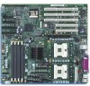
List of Figures Intel® Server Board SE7505VB2 List of Figures Figure 1. The Board Block Diagram 15 Figure 2. Memory Sub-system Block Diagram 18 Figure 3. Memory Bank Label Definition 20 Figure 4. SE7505VB2 Clock Distribution Diagram 32 Figure 5. Video Controller PCI Bus Interface 38 Figure 6. Interrupt Routing Diagram (ICH4 Internal 42 Figure 7. Interrupt Routing Diagram 43 Figure 8. The Board PCI Interrupt Mapping Diagram 44 Figure 9. Hardware Monitoring 47 Figure 10. System Recovery and Update Jumpers (J4J1 66 Figure 11. BIOS Recovery Jumper 92 Figure 12. Output Voltage Timing 97 Figure 13. Turn on / off Timing...98 Figure 14. Intel Server Board SE7505VB2 Mechanical Drawing 104 Figure 15. Board Photograph (Reference Only 105 viii Revision 1.2 Intel part number C32194-002

  • 1
  • 2
  • 3
  • 4
  • 5
  • 6
  • 7
  • 8
  • 9
  • 10
  • 11
  • 12
  • 13
  • 14
  • 15
  • 16
  • 17
  • 18
  • 19
  • 20
  • 21
  • 22
  • 23
  • 24
  • 25
  • 26
  • 27
  • 28
  • 29
  • 30
  • 31
  • 32
  • 33
  • 34
  • 35
  • 36
  • 37
  • 38
  • 39
  • 40
  • 41
  • 42
  • 43
  • 44
  • 45
  • 46
  • 47
  • 48
  • 49
  • 50
  • 51
  • 52
  • 53
  • 54
  • 55
  • 56
  • 57
  • 58
  • 59
  • 60
  • 61
  • 62
  • 63
  • 64
  • 65
  • 66
  • 67
  • 68
  • 69
  • 70
  • 71
  • 72
  • 73
  • 74
  • 75
  • 76
  • 77
  • 78
  • 79
  • 80
  • 81
  • 82
  • 83
  • 84
  • 85
  • 86
  • 87
  • 88
  • 89
  • 90
  • 91
  • 92
  • 93
  • 94
  • 95
  • 96
  • 97
  • 98
  • 99
  • 100
  • 101
  • 102
  • 103
  • 104
  • 105
  • 106
  • 107
  • 108

List of Figures
IntelĀ® Server Board SE7505VB2
List of Figures
Figure 1. The Board Block Diagram
............................................................................................
15
Figure 2. Memory Sub-system Block Diagram
............................................................................
18
Figure 3. Memory Bank Label Definition
.....................................................................................
20
Figure 4. SE7505VB2 Clock Distribution Diagram
......................................................................
32
Figure 5. Video Controller PCI Bus Interface
..............................................................................
38
Figure 6. Interrupt Routing Diagram (ICH4 Internal)
...................................................................
42
Figure 7. Interrupt Routing Diagram
...........................................................................................
43
Figure 8. The Board PCI Interrupt Mapping Diagram
.................................................................
44
Figure 9. Hardware Monitoring
...................................................................................................
47
Figure 10. System Recovery and Update Jumpers (J4J1)
.........................................................
66
Figure 11. BIOS Recovery Jumper
.............................................................................................
92
Figure 12. Output Voltage Timing
...............................................................................................
97
Figure 13. Turn on / off Timing
....................................................................................................
98
Figure 14. Intel Server Board SE7505VB2 Mechanical Drawing
..............................................
104
Figure 15. Board Photograph (Reference Only)
.......................................................................
105
Revision 1.2
Intel part number C32194-002
viii