JVC DLA-HX1U Instruction Manual - Page 58
Pin arrangement, Y/C terminal, RS-232C IN/OUT terminal, PC 1 terminal, Pin number, Signal name
 |
View all JVC DLA-HX1U manuals
Add to My Manuals
Save this manual to your list of manuals |
Page 58 highlights
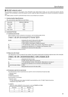
Specifications Pin arrangement Ⅵ Y/C terminal 4 3 2 1 Pin number 1 2 3 4 Signal name GND (Y) GND (C) Y C Ⅵ RS-232C IN/OUT terminal 9876 54321 Pin number 1 2 3 4 5 Signal name N/C RD TD N/C GND Pin number 6 7 8 9 Signal name N/C N/C N/C N/C N/C Ⅵ PC 1 terminal 11 12 13 14 15 6 7 1 2 8 3 4 5 9 10 Pin number 1 2 3 4 5 6 7 8 Signal name Red Green Blue N/C N/C GND (Red) GND (Green) GND (Blue) Pin number 9 10 11 12 13 14 15 Signal name N/C GND (SYNC) GND N/C H.SYNC V.SYNC N/C Ⅵ PC 3 terminal 8 7 65 4 3 2 1 16 15 14 13 12 11 10 9 24 23 22 21 20 19 18 17 58 Pin number Signal name Pin number 1 TMDS data 2 - 13 2 TMDS data 2 + 14 3 TMDS data 2/4 shield 15 4 N/C 16 5 N/C 17 6 DDC clock 18 7 DDC data 19 8 N/C 20 9 TMDS data 1 - 21 10 TMDS data 1 + 22 11 TMDS data 1/3 shield 23 12 N/C 24 TMDS = Transition Minimized Differential Signaling DDC = Display Data Channel Signal name N/C TMDS +5 V power supply Earth (+5 V) Hot plug detection TMDS data 0 TMDS data 0 + TMDS data 0/5 shield N/C N/C TMDS clock shield TMDS clock + TMDS clock -
-
 1
1 -
2
-
3
-
4
-
5
-
6
-
7
-
8
-
9
-
10
-
11
-
12
-
13
-
14
-
15
-
16
-
17
-
18
-
19
-
20
-
21
-
22
-
23
-
24
-
25
-
26
-
27
-
28
-
29
-
30
-
31
-
32
-
33
-
34
-
35
-
36
-
37
-
38
-
39
-
40
-
41
-
42
-
43
-
44
-
45
-
46
-
47
-
48
-
49
-
50
-
51
-
52
-
 53
53 -
 54
54 -
 55
55 -
 56
56 -
 57
57 -
 58
58 -
 59
59 -
 60
60 -
 61
61 -
 62
62
 |
 |