Dell 1815dn Service Manual - Page 22
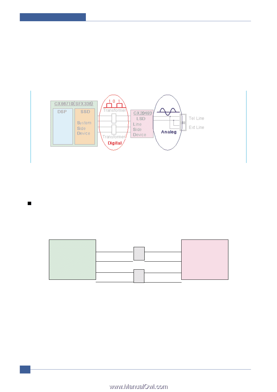
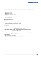
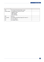
there is A/D, D/A Converter in LSD, so Analog Signal from Tel Line is converted in Digital through A/D
 |
UPC - 000061100008
View all Dell 1815dn manuals
Add to My Manuals
Save this manual to your list of manuals |
Page 22 highlights
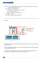
System Outline Signal Transition of DAA Solution Line Interface Signal of Tel Line and LSD is Analog Signal. 2) there is A/D, D/A Converter in LSD, so Analog Signal from Tel Line is converted in Digital through A/D Converter in DAA and transfer to SSD by DIB Capacitor Digital Signal from SSD is converted to Analog by D/A Converter in DAA and transfer to Tel Line Transformer transfer Clock from SSD to LSD and Clock Frequency is 4.032MHz. LSD full wave rectifies Clock to use as inner Power supply and also use as Main Clock for DIB Protocol Sync between LSD and SSD. Transformer transfer Clock by separating Primary and Secondary , and amplifies Clock Level to LSD by Coil Turns Ratio 1:1.16. Clock - Clock is supplied by transformer from SSD to LSD, and there is PWROUT to adjust output impedance of Clock CLKP SSD CLKN LSD DIBP DIBN Out Driver is inside SSD and CLKSHIGH Resistor to adjust duty of HLPWR Resistor and Clock. Clock from SSD to LSD has Dif ferential structure of 180 phase dif ference for Noise Robustness DIB Data transfer Data from SSD to LSD by Transformer, and also transfer specific data from LSD to SSD. After transferring data from SSD, RSP is transferred and LSD recognizes RSP and change LSD to output Driver transfer Data to SSD. DIB Data form SSD to LSD by Transformer has Differential structure of 180 phase dif ference between DIBP and DIBN for Noise Robustness 4-4 Service Manual
-
 1
1 -
2
-
3
-
4
-
5
-
6
-
7
-
8
-
9
-
10
-
11
-
12
-
13
-
14
-
15
-
16
-
 17
17 -
 18
18 -
 19
19 -
 20
20 -
 21
21 -
 22
22 -
 23
23 -
 24
24 -
 25
25 -
 26
26 -
 27
27 -
28
-
29
-
30
-
31
-
32
-
33
-
34
-
35
-
36
-
37
-
38
-
39
-
40
-
41
-
42
-
43
-
44
-
45
-
46
-
47
-
48
-
49
-
50
-
51
-
52
-
53
-
54
-
55
-
56
-
57
-
58
-
59
-
60
-
61
-
62
-
63
-
64
-
65
-
66
-
67
-
68
-
69
-
70
-
71
-
72
-
73
-
74
-
75
-
76
-
77
-
78
-
79
-
80
-
81
-
82
-
83
-
84
-
85
-
86
-
87
-
88
-
89
-
90
-
91
-
92
-
93
-
94
-
95
-
96
-
97
-
98
-
99
-
100
-
101
-
102
-
103
-
104
-
105
-
106
-
107
-
108
-
109
-
110
-
111
-
112
-
113
-
114
-
115
-
116
-
117
-
118
-
119
-
120
-
121
-
122
-
123
-
124
-
125
-
126
-
127
-
128
-
129
-
130
-
131
-
132
-
133
-
134
-
135
-
136
-
137
-
138
-
139
-
140
-
141
-
142
-
143
-
144
-
145
-
146
-
147
-
148
-
149
-
150
-
151
-
152
 |
 |