Epson 2070 Service Manual - Page 65
POWER SUPPLY OPERATION, Power Supply Output Voltages and Applications - driver lq
 |
UPC - 010343812277
View all Epson 2070 manuals
Add to My Manuals
Save this manual to your list of manuals |
Page 65 highlights
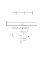
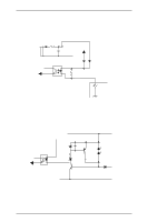
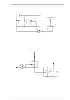
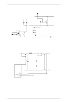
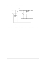
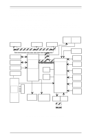
LQ-2070 Service Manual Operating Principles 2.2 POWER SUPPLY OPERATION The printer can be powered by either of two power supply boards: the C166 PSB (120 V) or C166 PSE (230 V) power supply. These boards are the same as the FX-2170. Additionally, the PSB and PSE boards function the same, except for a difference in primary circuitry. The power supply board outputs the DC current necessary to drive the printer control circuits and drive mechanism. Table 2-5 shows the input voltages and fuse ratings for these boards. Table 2-5. Power Supply Board Board C166 PSB C166 PSE Input Voltage 103.5 to 132 VAC 198 to 264 VAC Fuse F1 Rating 3.15 A / 125 V T2.0 AH / 250 V 2.2.1 Power Supply Overview The power supply board has two power outputs for use by the various control circuits and drive mechanisms. Table 2-6 lists the applications for the two DC output supply voltages. Table 2-6 Power Supply Output Voltages and Applications Output Voltage (DC) Applications +5 V Main Board Logic Circuit Sensors +35 V CR Motor PF Motor Figure 2-22 shows a block diagram of the power supply circuitry. Control Panel LEDs Printhead Driver Primary Circuit Secondary Circuit +5V Switching Regurator +5V Constant Voltage Control Circuit +5V Over current Protection Circuit +5V DC Full Wave Rectification Circuit Smoothing Circuit Filter Circuit AC input Switching Circuit Smoothing Circuit PhotoCoupler PhotoCoupler +35V Line Over Load Detector Circuit +35V Line Constant Voltage Control Circuit +35V Line Over Voltage Protection Circuit +5V Line Over Voltage Protection Circuit +35V Line Over Current Protection Circuit +35V DC CPU Port 20 Operation SW Figure 2- 22 Power Supply Circuit Block Diagram As shown in the figure above, when AC power enters the printer from an external power source, the filter circuit removes the noise. The AC voltage then undergoes full-wave rectification and is smoothed to produce direct voltage. The voltage is fed to the gate port for the switching FET (Q1: K2126 or K21230) through resistors R18 and R31, and then the switching circuit operates. The secondary smoothing circuit produces a stepped down +35 VDC voltage. The +5 VDC voltage is generated by feeding the +35 VDC voltage through the +5 VDC power supply circuit, where the +35 VDC is stepped down to a stable +5 VDC from the 35 VDC line. Rev.A 2-17
-
 1
1 -
2
-
3
-
4
-
5
-
6
-
7
-
8
-
9
-
10
-
11
-
12
-
13
-
14
-
15
-
16
-
17
-
18
-
19
-
20
-
21
-
22
-
23
-
24
-
25
-
26
-
27
-
28
-
29
-
30
-
31
-
32
-
33
-
34
-
35
-
36
-
37
-
38
-
39
-
40
-
41
-
42
-
43
-
44
-
45
-
46
-
47
-
48
-
49
-
50
-
51
-
52
-
53
-
54
-
55
-
56
-
57
-
58
-
59
-
 60
60 -
 61
61 -
 62
62 -
 63
63 -
 64
64 -
 65
65 -
 66
66 -
 67
67 -
 68
68 -
 69
69 -
 70
70 -
71
-
72
-
73
-
74
-
75
-
76
-
77
-
78
-
79
-
80
-
81
-
82
-
83
-
84
-
85
-
86
-
87
-
88
-
89
-
90
-
91
-
92
-
93
-
94
-
95
-
96
-
97
-
98
-
99
-
100
-
101
-
102
-
103
-
104
-
105
-
106
-
107
-
108
-
109
-
110
-
111
-
112
-
113
-
114
-
115
-
116
-
117
-
118
-
119
-
120
-
121
-
122
-
123
-
124
-
125
-
126
-
127
-
128
-
129
-
130
-
131
-
132
-
133
-
134
-
135
-
136
-
137
-
138
-
139
-
140
-
141
-
142
-
143
-
144
-
145
-
146
-
147
-
148
-
149
-
150
-
151
-
152
-
153
-
154
-
155
-
156
-
157
-
158
-
159
-
160
-
161
-
162
-
163
-
164
-
165
 |
 |