Epson 2070 Service Manual - Page 74
PF Motor Driver Circuit, 3.6 EEPROM Control Circuit,
 |
UPC - 010343812277
View all Epson 2070 manuals
Add to My Manuals
Save this manual to your list of manuals |
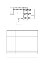
Page 74 highlights
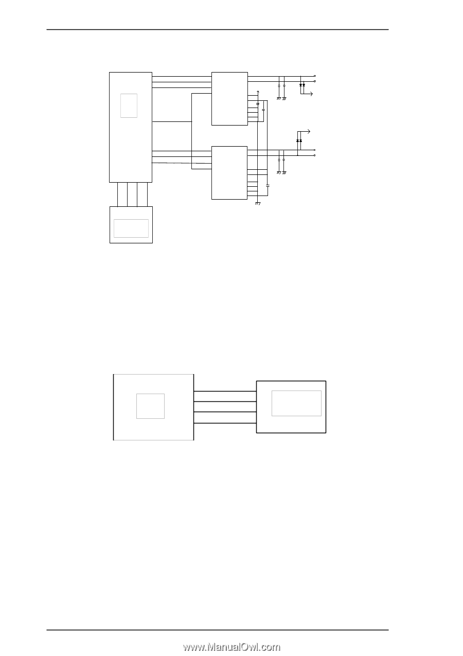
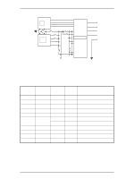
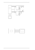
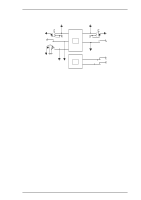
Operation Principles LQ-2070 Servcie Manual 2.3.5 PF Motor Driver Circuit The figure below shows the PF motor driver circuit. 63 PFI1A P FI 0A 62 PFFASEA 32 Gate Array IC2 66 PFHOLD IC11 9 7 IN0 IN1 8 PHASE 11 REF 15 OUTA OUTB 1 C66 3 VS1 VS2 14 C26 GND1 +35V GND2 GND3 GND4 65 PFI1B 64 PFI0B 129 PFFASEB PP PP PP PP G3 G2 G1 G0 7 8 9 10 876 5 PG PG PG PG 13 12 11 10 CPU IC1 IC14 9 IN0 7 IN1 8 PHASE 11 REF 15 OUTA OUTB 1 3 VS1 VS2 14 GND1 GND2 GND3 GND4 C66 C73 C67 D4 1 PF A 3 PF-A D5 +35 D6 C67 +35 D7 2 4 PF B PF-B Figure 2-36 PF Motor Driver Circuit The gate array receives phase data from the CPU via ports 7 (PPG3), 8 (PPG2), 9 (PPG1), and 10 (PPG0), converts the data to TEA3718SDP form, and then sends that phase data via ports 32 (PHASEA) and ports 129 (PHASEB) to each ports 8 (PHASE) of TEA3718SDP. The PF driver current is controlled on the Gate Array and the signals are output via port 62 (PFI0A), port 63 (PFI1A), port 64 (PFI0B), port 65 (PFI1B). These controlled drive currents are output to the each ports 9 (IN0), port 7 (IN1)of the TEA3718SDP. 2.3.6 EEPROM Control Circuit The EEPROM is non-volatile memory that stores information even if the printer power is off. The figure below shows the EEPROM control circuit. CPU 9 P70 P71 10 P72 11 12 P73 1 CS 2 CK 3 DI 4 DO IC 8 EEPROM Figure 2-37 EEPROM Control Circuit The EEPROM is controlled by CPU ports 9 (P70), 10 (P71), 11 (P72), and 12 (P73). Port 11 is the data output line used to save the information to the EEPROM, and port 12 is the data input line used to read the saved data from the EEPROM. Port 70 is the chip select line, and port 71 is the clock timing line. When the PWDN signal (power down) is detected on port 20 (INTO), the CPU writes the necessary data to the EEPROM before the +5 V line drops to 4.75 V. 2-26 Rev.A
-
 1
1 -
2
-
3
-
4
-
5
-
6
-
7
-
8
-
9
-
10
-
11
-
12
-
13
-
14
-
15
-
16
-
17
-
18
-
19
-
20
-
21
-
22
-
23
-
24
-
25
-
26
-
27
-
28
-
29
-
30
-
31
-
32
-
33
-
34
-
35
-
36
-
37
-
38
-
39
-
40
-
41
-
42
-
43
-
44
-
45
-
46
-
47
-
48
-
49
-
50
-
51
-
52
-
53
-
54
-
55
-
56
-
57
-
58
-
59
-
60
-
61
-
62
-
63
-
64
-
65
-
66
-
67
-
68
-
 69
69 -
 70
70 -
 71
71 -
 72
72 -
 73
73 -
 74
74 -
 75
75 -
 76
76 -
 77
77 -
 78
78 -
 79
79 -
80
-
81
-
82
-
83
-
84
-
85
-
86
-
87
-
88
-
89
-
90
-
91
-
92
-
93
-
94
-
95
-
96
-
97
-
98
-
99
-
100
-
101
-
102
-
103
-
104
-
105
-
106
-
107
-
108
-
109
-
110
-
111
-
112
-
113
-
114
-
115
-
116
-
117
-
118
-
119
-
120
-
121
-
122
-
123
-
124
-
125
-
126
-
127
-
128
-
129
-
130
-
131
-
132
-
133
-
134
-
135
-
136
-
137
-
138
-
139
-
140
-
141
-
142
-
143
-
144
-
145
-
146
-
147
-
148
-
149
-
150
-
151
-
152
-
153
-
154
-
155
-
156
-
157
-
158
-
159
-
160
-
161
-
162
-
163
-
164
-
165
 |
 |