Epson 2070 Service Manual - Page 71
Table 2-7, Functions of the Main Board, Data Flow, Location, Function, Rev.A - lq drivers
 |
UPC - 010343812277
View all Epson 2070 manuals
Add to My Manuals
Save this manual to your list of manuals |
Page 71 highlights
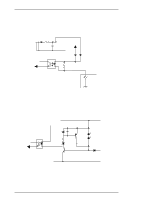
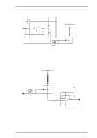
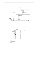
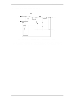
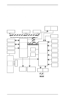
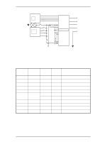
LQ-2070 Service Manual Operating Principles The following figure shows the data flow from the host computer to the printhead. Data sent from the host computer is converted to image data and transmitted to the printhead through the gate array. Option I/F Parallel I/F Host Computer CPU TMP96C041AF Gate Array E05B24YA Data latch and data output Print data conversion 1 Print data conversion 2 RAM Input Buffer Line Edit Buffer Image Buffer Image data transfer Printhead drive circuite Figure 2-31 Data Flow The following table lists the each function of the main components of the C186 MAIN board. Table 2-7 Functions of the Main Board IC Location Function CPU Receives data from the host computer and sends it to the input buffer in RAM (under interrupt processing control). Extends the input data IC1 held in the buffer to create image data. Loads this image data to the image buffer in RAM. Transfers the image data to the printhead driver circuit. Gate Array Controls the functions below: • Controls output data from the internal block • Memory management • Address latch of the address/data bus from the CPU IC2 • Clock control unit • Bit manipulation • Interface control • Expanded parallel port • Printhead control • Motor control EEPROM IC 8 An electrically writable and erasable ROM used to hold information such as the TOF position and bidirectional adjustment value. ROM IC 3 The ROM contains the program that runs the CPU and holds the character design (also called the character generator). RAM IC 5 The RAM contains the CPU working area and the buffers CG IC 7 The CG contains the bitmap fonts for each character table SLA7024M IC 12 Driver circuit for the CR motor TEA3718SDP IC 11,14 Driver circuit for the PF motor Rev.A 2-23
-
 1
1 -
2
-
3
-
4
-
5
-
6
-
7
-
8
-
9
-
10
-
11
-
12
-
13
-
14
-
15
-
16
-
17
-
18
-
19
-
20
-
21
-
22
-
23
-
24
-
25
-
26
-
27
-
28
-
29
-
30
-
31
-
32
-
33
-
34
-
35
-
36
-
37
-
38
-
39
-
40
-
41
-
42
-
43
-
44
-
45
-
46
-
47
-
48
-
49
-
50
-
51
-
52
-
53
-
54
-
55
-
56
-
57
-
58
-
59
-
60
-
61
-
62
-
63
-
64
-
65
-
 66
66 -
 67
67 -
 68
68 -
 69
69 -
 70
70 -
 71
71 -
 72
72 -
 73
73 -
 74
74 -
 75
75 -
 76
76 -
77
-
78
-
79
-
80
-
81
-
82
-
83
-
84
-
85
-
86
-
87
-
88
-
89
-
90
-
91
-
92
-
93
-
94
-
95
-
96
-
97
-
98
-
99
-
100
-
101
-
102
-
103
-
104
-
105
-
106
-
107
-
108
-
109
-
110
-
111
-
112
-
113
-
114
-
115
-
116
-
117
-
118
-
119
-
120
-
121
-
122
-
123
-
124
-
125
-
126
-
127
-
128
-
129
-
130
-
131
-
132
-
133
-
134
-
135
-
136
-
137
-
138
-
139
-
140
-
141
-
142
-
143
-
144
-
145
-
146
-
147
-
148
-
149
-
150
-
151
-
152
-
153
-
154
-
155
-
156
-
157
-
158
-
159
-
160
-
161
-
162
-
163
-
164
-
165
 |
 |
