Epson FX-85 User Manual - Page 88
ground level. For the interface wiring, be sure to use a twisted-pair
 |
View all Epson FX-85 manuals
Add to My Manuals
Save this manual to your list of manuals |
Page 88 highlights
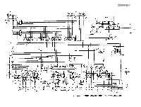
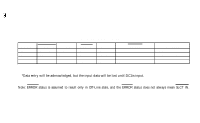
Table K-1, continued Signal Return Signal 13 -- 14 - AUTO FEED XT 15 - 16 - 17 - 18 - 19 - 30 - 31 - NC OV CHASSIS GND NC GND INIT 32 - ERROR 33 - GND 34 - NC 35 - - 36 - SLCT IN Direction Description - Pulled up to + 5 volts through 3.3K ohm resistance. When this signal is LOW, the paper is IN automatically fed 1 line after printing. (The signal level can be fixed to this by setting DIP switch 2-4 to ON.) - Unused. - Logic ground level. Printer's chassis ground, which is - isolated from the logic ground. - Unused. - Twisted-pair return signal ground level. IN When this level becomes LOW, the printer controller is reset to its powerup state and the print buffer is cleared. This level is usually High; its pulse width must be more than 50 microseconds at the receiving terminal. OUT This level becomes LOW when the printer is in: 1) Paper-end state. 2) Off-line. 3) Error state. - Same as for Pins 19 - 30. - Unused. - Pulled up to + 5V through 3.3K ohm resistance. IN Data entry to the printer is possible only when this level is LOW; DIP switch 2-1 is set for this at the factory Notes: 1. The column heading "Direction" refers to the direction of signal flow as viewed from the printer. 2. "Return" denotes the twisted-pair return, to be connected at signal ground level. For the interface wiring, be sure to use a twisted-pair cable for each signal and to complete the connection on the return side. To prevent noise, these cables should be shielded and connected to the chassis of the host computer or the printer. 3. All interface conditions are based on TTL level. Both the rise and the fall times of each signal must be less than 0.2 microseconds. 334
-
 1
1 -
2
-
3
-
4
-
5
-
6
-
7
-
8
-
9
-
10
-
11
-
12
-
13
-
14
-
15
-
16
-
17
-
18
-
19
-
20
-
21
-
22
-
23
-
24
-
25
-
26
-
27
-
28
-
29
-
30
-
31
-
32
-
33
-
34
-
35
-
36
-
37
-
38
-
39
-
40
-
41
-
42
-
43
-
44
-
45
-
46
-
47
-
48
-
49
-
50
-
51
-
52
-
53
-
54
-
55
-
56
-
57
-
58
-
59
-
60
-
61
-
62
-
63
-
64
-
65
-
66
-
67
-
68
-
69
-
70
-
71
-
72
-
73
-
74
-
75
-
76
-
77
-
78
-
79
-
80
-
81
-
82
-
 83
83 -
 84
84 -
 85
85 -
 86
86 -
 87
87 -
 88
88 -
 89
89 -
 90
90 -
 91
91 -
 92
92 -
 93
93 -
94
-
95
-
96
-
97
-
98
-
99
-
100
-
101
-
102
-
103
-
104
-
105
-
106
-
107
-
108
 |
 |