Pioneer PDP-425CMX User Manual - Page 49
Appendix 2: INPUT1/2 pin assignments
 |
View all Pioneer PDP-425CMX manuals
Add to My Manuals
Save this manual to your list of manuals |
Page 49 highlights
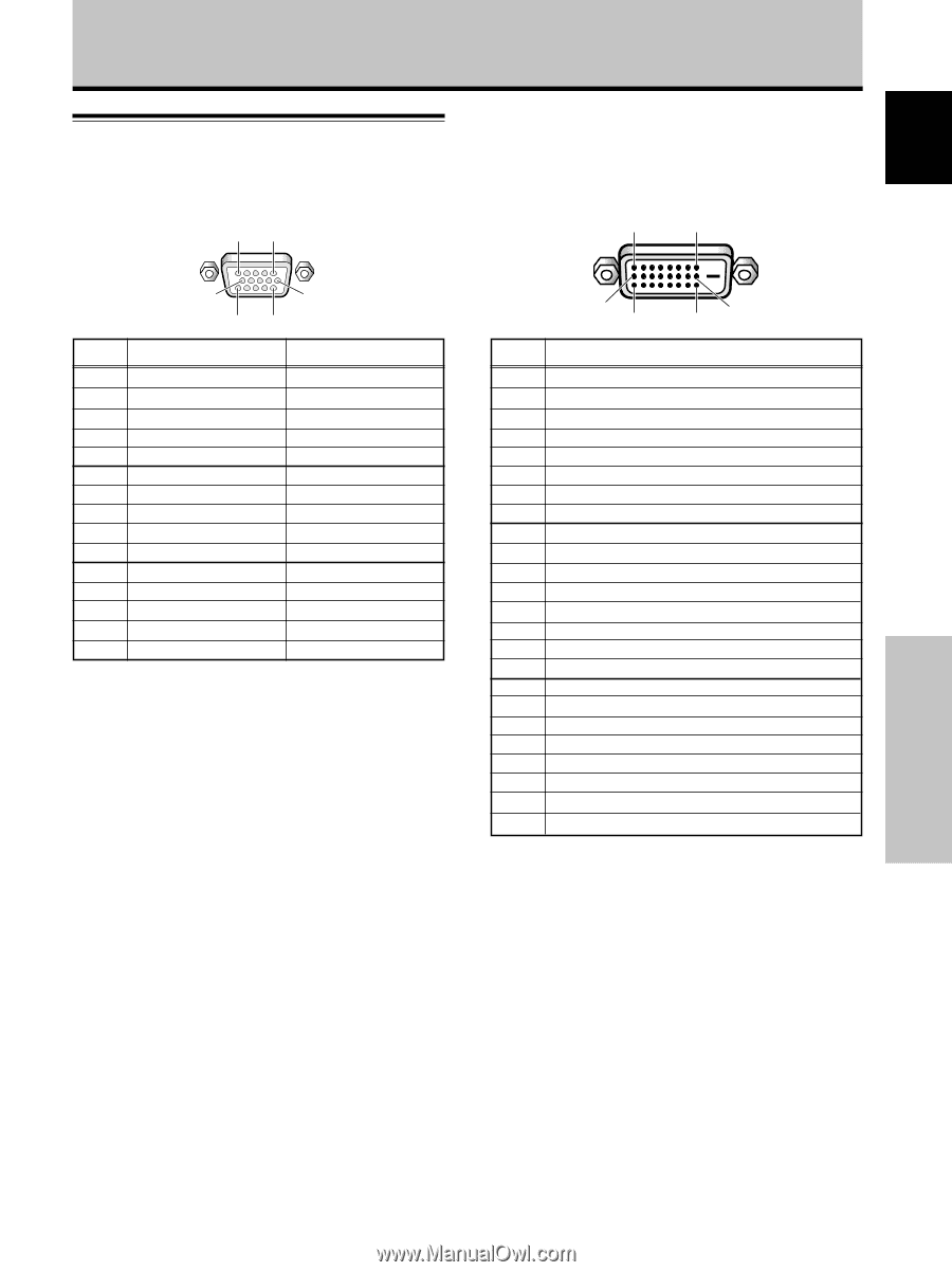
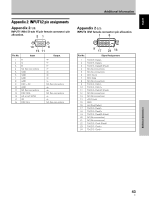
English Additional Information Appendix 2: INPUT1/2 pin assignments Appendix 2-1/2: INPUT1 (Mini D-sub 15 pin female connector) pin allocation. 51 Appendix 2-2/2: INPUT2 (DVI female connector) pin allocation. 1 8 10 6 15 11 Pin No. Input Output 1R 2G 3B 4 NC (No connection) 5 GND 6 GND 7 GND 8 GND 9 DDC + 5V 10 GND 11 NC (No connection) 12 DDC SDA 13 HD or H/V SYNC 14 VD 15 DDC SCL NC (No connection) + + NC (No connection) + + NC (No connection) 9 17 24 16 Pin No. Signal Assignment 1 T.M.D.S. Data2- 2 T.M.D.S. Data2+ 3 T.M.D.S. Data2/4 Shield 4 NC (No connection) 5 NC (No connection) 6 DDC Clock 7 DDC Data 8 NC (No connection) 9 T.M.D.S. Data1- 10 T.M.D.S. Data1+ 11 T.M.D.S. Data1/3 Shield 12 NC (No connection) 13 NC (No connection) 14 +5V Power 15 GND 16 Hot Plug Detect 17 T.M.D.S. Data0 - 18 T.M.D.S. Data0 + 19 T.M.D.S. Data0/5 Shield 20 NC (No connection) 21 NC (No connection) 22 T.M.D.S. Clock Shield 23 T.M.D.S. Clock+ 24 T.M.D.S. Clock- Additional Information 43 En
-
 1
1 -
2
-
3
-
4
-
5
-
6
-
7
-
8
-
9
-
10
-
11
-
12
-
13
-
14
-
15
-
16
-
17
-
18
-
19
-
20
-
21
-
22
-
23
-
24
-
25
-
26
-
27
-
28
-
29
-
30
-
31
-
32
-
33
-
34
-
35
-
36
-
37
-
38
-
39
-
40
-
41
-
42
-
43
-
 44
44 -
 45
45 -
 46
46 -
 47
47 -
 48
48 -
 49
49 -
 50
50 -
 51
51 -
 52
52 -
 53
53 -
 54
54 -
55
-
56
-
57
-
58
-
59
-
60
-
61
-
62
-
63
-
64
-
65
-
66
-
67
-
68
-
69
-
70
-
71
-
72
-
73
-
74
-
75
-
76
-
77
-
78
-
79
-
80
-
81
-
82
-
83
-
84
-
85
-
86
-
87
-
88
-
89
-
90
-
91
-
92
-
93
-
94
-
95
-
96
-
97
-
98
 |
 |