Intel D845PEBT2 Product Specification - Page 15
Block Diagram - sata
 |
View all Intel D845PEBT2 manuals
Add to My Manuals
Save this manual to your list of manuals |
Page 15 highlights
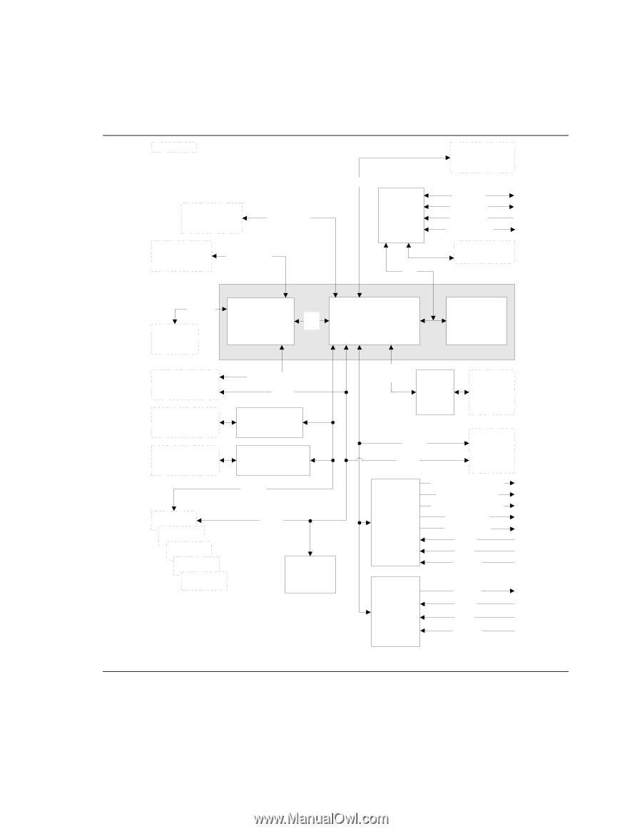
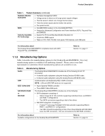
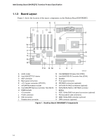
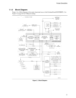
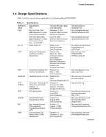
Product Description 1.1.4 Block Diagram Figure 2 is a block diagram of the major functional areas of the Desktop Board D845PEBT2. See Figure 4 on page 24 for USB port routing. = connector or socket Primary/ Secondary IDE UDMA 33 and ATA-66/100 mPGA478 Processor Socket System Bus (400/533 MHz) USB LPC Bus I/O Controller LPC Bus Back Panel/ Front Panel USB Ports Serial Port Parallel Port PS/2 Mouse PS/2 Keyboard Diskette Drive Connector AGP Interface 4X AGP Connector (1.5 V only) Intel 82845PE Memory Controller Hub (MCH) AHA Bus Two DIMM Banks Primary/Secondary SATA/SATA RAID or IDE RAID Three IEEE 1394a-2000 Ports (Optional) Memory Bus SMBus SATA/SATA RAID or IDE RAID Controller FW323 IEEE 1394a-2000 Controller (Optional) PCI Bus PCI Slot 1 PCI Slot 2 PCI Slot 3 PCI Slot 4 PCI Slot 5 SMBus Hardware Monitoring and Fan Control ASIC Intel 82801DB I/O Controller Hub (ICH4) Intel 82802AB 4 Mbit Firmware Hub (FWH) Intel 845PE Chipset CSMA/CD Unit Interface Physical Layer Interface LAN Connector AC Link SMBus CNR Connector (Optional) AD1980 Audio Codec (Optional) Front Left and Right Out Center and LFE Out Rear Left and Right Out Digital S/PDIF Optical S/PDIF Line In Mic In CD-ROM AD1981B Audio Codec (Optional) Line Out Line In Mic In CD-ROM Figure 2. Block Diagram OM15028 15
-
 1
1 -
2
-
3
-
4
-
5
-
6
-
7
-
8
-
9
-
 10
10 -
 11
11 -
 12
12 -
 13
13 -
 14
14 -
 15
15 -
 16
16 -
 17
17 -
 18
18 -
 19
19 -
 20
20 -
21
-
22
-
23
-
24
-
25
-
26
-
27
-
28
-
29
-
30
-
31
-
32
-
33
-
34
-
35
-
36
-
37
-
38
-
39
-
40
-
41
-
42
-
43
-
44
-
45
-
46
-
47
-
48
-
49
-
50
-
51
-
52
-
53
-
54
-
55
-
56
-
57
-
58
-
59
-
60
-
61
-
62
-
63
-
64
-
65
-
66
-
67
-
68
-
69
-
70
-
71
-
72
-
73
-
74
-
75
-
76
-
77
-
78
-
79
-
80
-
81
-
82
-
83
-
84
-
85
-
86
-
87
-
88
-
89
-
90
-
91
-
92
-
93
-
94
-
95
-
96
-
97
-
98
-
99
-
100
-
101
-
102
-
103
-
104
-
105
-
106
-
107
-
108
-
109
-
110
-
111
-
112
-
113
-
114
-
115
-
116
-
117
-
118
-
119
-
120
-
121
-
122
-
123
-
124
-
125
-
126
-
127
-
128
 |
 |