Intel D845PEBT2 Product Specification - Page 63
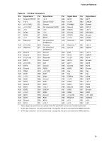
Table 37., PCI Bus Connectors
 |
View all Intel D845PEBT2 manuals
Add to My Manuals
Save this manual to your list of manuals |
Page 63 highlights
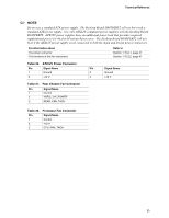
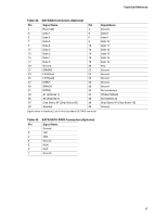
Technical Reference Table 37. PCI Bus Connectors Pin Signal Name Pin Signal Name Pin Signal Name A1 Ground (TRST#)* B1 -12 V A32 AD16 A2 +12 V B2 Ground (TCK)* A33 +3.3 V A3 +5 V (TMS)* B3 Ground A34 FRAME# A4 +5 V (TDI)* B4 Not connected (TDO)* A35 Ground A5 +5 V B5 +5 V A36 TRDY# A6 INTA# B6 +5 V A37 Ground A7 INTC# B7 INTB# A38 STOP# A8 +5 V B8 INTD# A39 +3.3 V A9 Reserved B9 Not connected (PRSNT1#)* A40 Reserved ** Pin Signal Name B32 AD17 B33 C/BE2# B34 Ground B35 IRDY# B36 +3.3 V B37 DEVSEL# B38 Ground B39 LOCK# B40 PERR# A10 +5 V (I/O) B10 Reserved A41 Reserved *** B41 +3.3 V A11 Reserved B11 Not connected (PRSNT2#)* A42 Ground B42 SERR# A12 Ground B12 Ground A43 PAR B43 +3.3 V A13 Ground B13 Ground A44 AD15 B44 C/BE1# A14 +3.3 V aux B14 Reserved A45 +3.3 V B45 AD14 A15 RST# B15 Ground A46 AD13 B46 Ground A16 +5 V (I/O) B16 CLK A47 AD11 B47 AD12 A17 GNT# B17 Ground A48 Ground B48 AD10 A18 Ground B18 REQ# A49 AD09 B49 Ground A19 PME# B19 +5 V (I/O) A50 Key B50 Key A20 AD30 B20 AD31 A51 Key B51 Key A21 +3.3 V B21 AD29 A52 C/BE0# B52 AD08 A22 AD28 B22 Ground A53 +3.3 V B53 AD07 A23 AD26 B23 AD27 A54 AD06 B54 +3.3 V A24 Ground B24 AD25 A55 AD04 B55 AD05 A25 AD24 B25 +3.3 V A56 Ground B56 AD03 A26 IDSEL B26 C/BE3# A57 AD02 B57 Ground A27 +3.3 V A28 AD22 A29 AD20 A30 Ground A31 AD18 B27 AD23 B28 Ground B29 AD21 B30 AD19 B31 +3.3 V A58 AD00 A59 +5 V (I/O) A60 REQ64# A61 +5 V A62 +5 V B58 AD01 B59 +5 V (I/O) B60 ACK64# B61 +5 V B62 +5 V * These signals (in parentheses) are optional in the PCI specification and are not currently implemented. ** On PCI bus connector 1 or 2 (see section 2.8.2.1 on page 57), this pin is connected to the SMBus clock line. *** On PCI bus connector 1 or 2 (see section 2.8.2.1 on page 57), this pin is connected to the SMBus data line. 63
-
 1
1 -
2
-
3
-
4
-
5
-
6
-
7
-
8
-
9
-
10
-
11
-
12
-
13
-
14
-
15
-
16
-
17
-
18
-
19
-
20
-
21
-
22
-
23
-
24
-
25
-
26
-
27
-
28
-
29
-
30
-
31
-
32
-
33
-
34
-
35
-
36
-
37
-
38
-
39
-
40
-
41
-
42
-
43
-
44
-
45
-
46
-
47
-
48
-
49
-
50
-
51
-
52
-
53
-
54
-
55
-
56
-
57
-
 58
58 -
 59
59 -
 60
60 -
 61
61 -
 62
62 -
 63
63 -
 64
64 -
 65
65 -
 66
66 -
 67
67 -
 68
68 -
69
-
70
-
71
-
72
-
73
-
74
-
75
-
76
-
77
-
78
-
79
-
80
-
81
-
82
-
83
-
84
-
85
-
86
-
87
-
88
-
89
-
90
-
91
-
92
-
93
-
94
-
95
-
96
-
97
-
98
-
99
-
100
-
101
-
102
-
103
-
104
-
105
-
106
-
107
-
108
-
109
-
110
-
111
-
112
-
113
-
114
-
115
-
116
-
117
-
118
-
119
-
120
-
121
-
122
-
123
-
124
-
125
-
126
-
127
-
128
 |
 |