Intel D845PEBT2 Product Specification - Page 61
Add-in Board and Peripheral Interface Connectors
 |
View all Intel D845PEBT2 manuals
Add to My Manuals
Save this manual to your list of manuals |
Page 61 highlights
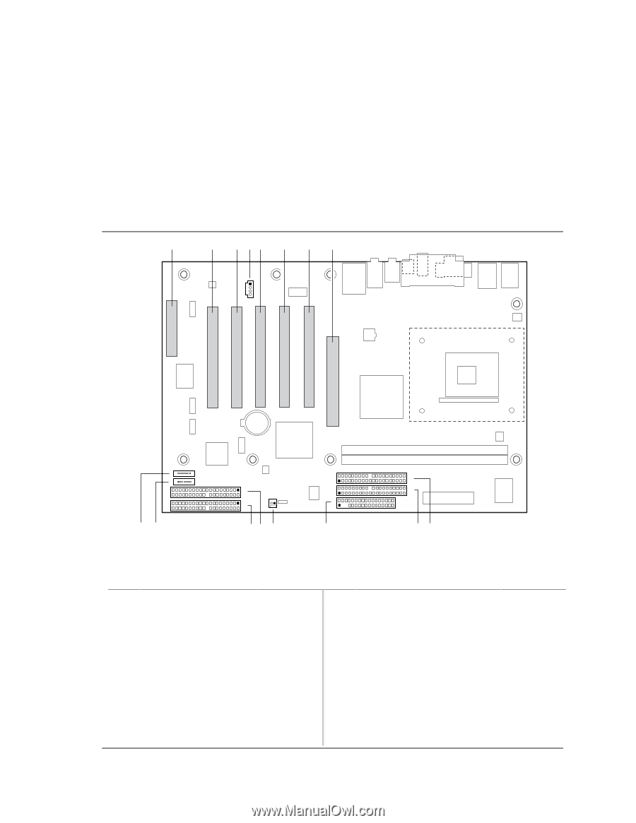
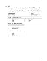
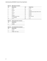
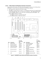
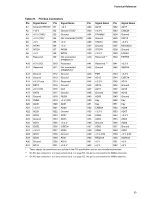
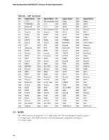
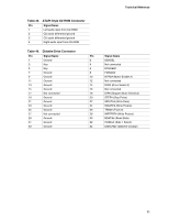
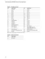
Technical Reference 2.8.2.3 Add-in Board and Peripheral Interface Connectors Figure 14 shows the location of the add-in board and peripheral connectors for the Desktop Board D845PEBT2. Note the following considerations for the PCI bus connectors: • All of the PCI bus connectors are bus master capable. • The SMBus is routed to PCI bus connector 1 or 2 depending on the board's AA number labeled on the board's front right corner (see section 2.8.2.1 on page 57). This enables PCI bus add-in boards with SMBus support to access sensor data on the Desktop Board D845PEBT2. The specific SMBus signals are as follows: The SMBus clock line is connected to pin A40 The SMBus data line is connected to pin A41 A B C DE F G H 1 4 7 1 2 1 7 1 39 40 1 2 1 2 1 39 1 40 2 2 1 40 39 40 39 34 33 PO NM L K JI Item A B C D E Description CNR (optional) PCI bus connector 5 PCI bus connector 4 ATAPI-style CD-ROM PCI bus connector 3 F PCI bus connector 2 G PCI bus connector 1 H AGP For more information see: Table 36 Table 37 Table 39 Table 37 Table 37 Table 37 Table 37 Table 38 Item I J K L M N O P Description Secondary IDE [white] Primary IDE [black] Diskette drive SCSI LED Secondary IDE RAID [blue] (optional) Primary IDE RAID [blue] (optional) Primary SATA/SATA RAID (optional) Secondary SATA/SATA RAID (optional) OM15034 For more information see: Table 41 Table 41 Table 40 Table 42 Table 43 Table 43 Table 44 Table 44 Figure 14. D845PEBT2 Add-in Board and Peripheral Interface Connectors 61
-
 1
1 -
2
-
3
-
4
-
5
-
6
-
7
-
8
-
9
-
10
-
11
-
12
-
13
-
14
-
15
-
16
-
17
-
18
-
19
-
20
-
21
-
22
-
23
-
24
-
25
-
26
-
27
-
28
-
29
-
30
-
31
-
32
-
33
-
34
-
35
-
36
-
37
-
38
-
39
-
40
-
41
-
42
-
43
-
44
-
45
-
46
-
47
-
48
-
49
-
50
-
51
-
52
-
53
-
54
-
55
-
 56
56 -
 57
57 -
 58
58 -
 59
59 -
 60
60 -
 61
61 -
 62
62 -
 63
63 -
 64
64 -
 65
65 -
 66
66 -
67
-
68
-
69
-
70
-
71
-
72
-
73
-
74
-
75
-
76
-
77
-
78
-
79
-
80
-
81
-
82
-
83
-
84
-
85
-
86
-
87
-
88
-
89
-
90
-
91
-
92
-
93
-
94
-
95
-
96
-
97
-
98
-
99
-
100
-
101
-
102
-
103
-
104
-
105
-
106
-
107
-
108
-
109
-
110
-
111
-
112
-
113
-
114
-
115
-
116
-
117
-
118
-
119
-
120
-
121
-
122
-
123
-
124
-
125
-
126
-
127
-
128
 |
 |