LG 50PJ340 Training Manual - Page 93
Control Board LVDS P121 Connector Voltages and Diode Check
 |
View all LG 50PJ340 manuals
Add to My Manuals
Save this manual to your list of manuals |
Page 93 highlights
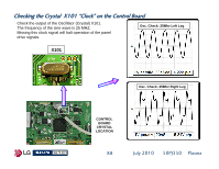
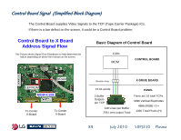
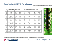
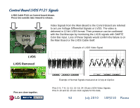
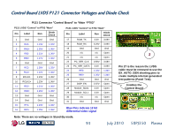
Control Board LVDS P121 Connector Voltages and Diode Check P121 Connector "Control Board" to "Main "P703" P121 LVDS "Control" to P703 "Main" Pin Label Run Diode Check 1 Gnd Gnd Gnd 2 RA2- 1.13V 1.32V 3 RA2+ 1.35V 1.36V 4 RB2- 1.21V 1.36V 5 RB2+ 1.27V 1.36V 6 Gnd Gnd Gnd 7 RC2- 1.26V 1.32V 8 RC2+ 1.22V 1.36V 9 RCLK2- 1.23V 1.36V 10 RCLK2+ 1.23V 1.36V 11 RD2- 1.21V 1.36V 12 RD2+ 1.26V 1.36V 13 Gnd Gnd Gnd 14 Gnd Gnd Gnd 15 RF2- 1.23V 1.32V 16 RF2+ 1.25V 1.36V P121 LVDS "Control" to P703 "Main" Pin Label Run Diode Check 17 ROM_TX 3.3V 3.09V 18 ROM_RX 3.29V 3.09V 19 Gnd Gnd Gnd 20 n/c n/c Open 21 n/c n/c Open 22 PC_SER_CLK 0.59V 3.08V 23 PC_SER_DATA 3.3V 3.09V 24 RE2- 1.23V 1.36V 25 RE2+ 1.25V 1.36V 26 Gnd Gnd Gnd 27 DISP_EN 2.87V Open 28 Module_SDA1 3.3V Open 29 Module_SCL1 3.3V Open 30 n/c n/c Open 31 Gnd Gnd Gnd Blue Pins indicate 12 bit differential video signal 1 Pin 27 is the reason the LVDS cable must be removed to use the EX_AUTO_GEN shorting pins to create multiple internal generated test patterns (Panel Test). Enables the Control Board Note: There are no voltages in Stand-By mode. 93 July 2010 50PJ350 Plasma
-
 1
1 -
2
-
3
-
4
-
5
-
6
-
7
-
8
-
9
-
10
-
11
-
12
-
13
-
14
-
15
-
16
-
17
-
18
-
19
-
20
-
21
-
22
-
23
-
24
-
25
-
26
-
27
-
28
-
29
-
30
-
31
-
32
-
33
-
34
-
35
-
36
-
37
-
38
-
39
-
40
-
41
-
42
-
43
-
44
-
45
-
46
-
47
-
48
-
49
-
50
-
51
-
52
-
53
-
54
-
55
-
56
-
57
-
58
-
59
-
60
-
61
-
62
-
63
-
64
-
65
-
66
-
67
-
68
-
69
-
70
-
71
-
72
-
73
-
74
-
75
-
76
-
77
-
78
-
79
-
80
-
81
-
82
-
83
-
84
-
85
-
86
-
87
-
 88
88 -
 89
89 -
 90
90 -
 91
91 -
 92
92 -
 93
93 -
 94
94 -
 95
95 -
 96
96 -
 97
97 -
 98
98 -
99
-
100
-
101
-
102
-
103
-
104
-
105
-
106
-
107
-
108
-
109
-
110
-
111
-
112
-
113
-
114
-
115
-
116
-
117
-
118
-
119
-
120
-
121
-
122
-
123
-
124
-
125
-
126
-
127
-
128
-
129
-
130
-
131
-
132
-
133
 |
 |
