Epson Stylus Pro 7600 - UltraChrome Ink Service Manual - Page 93
Nibble Mode
 |
View all Epson Stylus Pro 7600 - UltraChrome Ink manuals
Add to My Manuals
Save this manual to your list of manuals |
Page 93 highlights
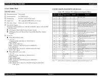
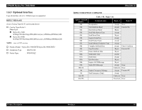
EPSON Stylus Pro 7600/9600 1.6.1.2 Nibble Mode SPECIFICATION † Transmission mode: 8 bit parallel † Synchronization: By STROBE pulse † Handshaking: By BUSY and ACKNLG signal † Signal level: TTL compatible (IEEE1284Level 1 device) † Data trans. timing: Refer to the IEEE-1284 specification † Extensibility Request: The printer responds affirmatively when the extensibility request values are 00H or 04H, that mean, „ 00H Request Nibble Mode Reverse Channel Transfer. „ 04H Request Device ID; Return Data Using Nibble Mode Rev Channel Transfer. † Device ID: „ When IEEE1284.4 is valid • (Character strings, depending on ) • MFG: EPSON; • CMD: ESCPL2,BDC,D4; • MDL: ; • CLS: PRINTER; • DES: EPSON;(:space) „ When IEEE1284.4 is not valid • (Character strings, depending on ) • MFG: EPSON; • CMD: ESCPL2,BDC; • MDL: ; • CLS: PRINTER; • DES: EPSONT; (:space) Revision A CONNECTOR PIN ASSIGNMENT AND SIGNALS Pin No. 1 2 3 4 5 6 7 8 9 10 11 12 13 14 31 32 36 18 35 17 16,33, 19-30 15,34 Table 1-55. Connector Pin Assignment and Signals (Nibble) Return GND Pin Signal Name 19 HostClk 20 DATA0 21 DATA1 22 DATA2 23 DATA3 24 DATA4 25 DATA5 26 DATA6 27 DATA7 28 PtrClk 29 PtrBusy /DataBit-3,7 28 AckDataReq /DataBit-2,6 28 Xflag /DataBit-1,5 30 HostBusy 30 -INIT 29 -DataAvail /DataBit-0,4 30 1284-Active -- Logic H -- +5V -- Chassis GND In/Out * Function In Host clock signal. In In In The DATA0 through DATA7 signals In represent data bits 0 to 7, respectively. Each In signal is at high level when data is logical 1 In and low level when data is logical 0. In In Out Printer clock signal. Out Printer busy signal and reverse channel transfer data bit 3 or 7. Out Acknowledge data request signal and reverse channel transfer data bit 2 or 6. Out X-flag signal and reverse channel transfer data bit 1 or 5. In Host busy signal. In Not used. Out Data available signal and reverse channel transfer data bit 0 or 4. In 1284 active signal. Out Always "HIGH". Pulled up to +5 V via 3.9 K ohm resistor. Out Always "HIGH". Pulled up to +5 V via 1.0 K ohm resistor. -- Chassis GND. -- GND -- Signal GND. -- NC -- Not used Note "*": In/Out refers to the direction of signal flow from the printer's point of view. Product Description Interfaces 93
-
 1
1 -
2
-
3
-
4
-
5
-
6
-
7
-
8
-
9
-
10
-
11
-
12
-
13
-
14
-
15
-
16
-
17
-
18
-
19
-
20
-
21
-
22
-
23
-
24
-
25
-
26
-
27
-
28
-
29
-
30
-
31
-
32
-
33
-
34
-
35
-
36
-
37
-
38
-
39
-
40
-
41
-
42
-
43
-
44
-
45
-
46
-
47
-
48
-
49
-
50
-
51
-
52
-
53
-
54
-
55
-
56
-
57
-
58
-
59
-
60
-
61
-
62
-
63
-
64
-
65
-
66
-
67
-
68
-
69
-
70
-
71
-
72
-
73
-
74
-
75
-
76
-
77
-
78
-
79
-
80
-
81
-
82
-
83
-
84
-
85
-
86
-
87
-
 88
88 -
 89
89 -
 90
90 -
 91
91 -
 92
92 -
 93
93 -
 94
94 -
 95
95 -
 96
96 -
 97
97 -
 98
98 -
99
-
100
-
101
-
102
-
103
-
104
-
105
-
106
-
107
-
108
-
109
-
110
-
111
-
112
-
113
-
114
-
115
-
116
-
117
-
118
-
119
-
120
-
121
-
122
-
123
-
124
-
125
-
126
-
127
-
128
-
129
-
130
-
131
-
132
-
133
-
134
-
135
-
136
-
137
-
138
-
139
-
140
-
141
-
142
-
143
-
144
-
145
-
146
-
147
-
148
-
149
-
150
-
151
-
152
-
153
-
154
-
155
-
156
-
157
-
158
-
159
-
160
-
161
-
162
-
163
-
164
-
165
-
166
-
167
-
168
-
169
-
170
-
171
-
172
-
173
-
174
-
175
-
176
-
177
-
178
-
179
-
180
-
181
-
182
-
183
-
184
-
185
-
186
-
187
-
188
-
189
-
190
-
191
-
192
-
193
-
194
-
195
-
196
-
197
-
198
-
199
-
200
-
201
-
202
-
203
-
204
-
205
-
206
-
207
-
208
-
209
-
210
-
211
-
212
-
213
-
214
-
215
-
216
-
217
-
218
-
219
-
220
-
221
-
222
-
223
-
224
-
225
-
226
-
227
-
228
-
229
-
230
-
231
-
232
-
233
-
234
-
235
-
236
-
237
-
238
-
239
-
240
-
241
-
242
-
243
-
244
-
245
-
246
-
247
-
248
-
249
-
250
-
251
-
252
-
253
-
254
-
255
-
256
-
257
-
258
-
259
-
260
-
261
-
262
-
263
-
264
-
265
-
266
-
267
-
268
-
269
-
270
-
271
-
272
-
273
-
274
-
275
-
276
-
277
-
278
-
279
-
280
-
281
-
282
-
283
-
284
-
285
-
286
-
287
-
288
-
289
-
290
-
291
-
292
-
293
-
294
-
295
-
296
-
297
-
298
-
299
-
300
-
301
-
302
-
303
-
304
-
305
-
306
-
307
-
308
-
309
-
310
-
311
-
312
-
313
-
314
-
315
-
316
-
317
-
318
-
319
-
320
-
321
-
322
-
323
-
324
-
325
-
326
-
327
-
328
-
329
-
330
-
331
-
332
-
333
-
334
-
335
-
336
 |
 |