Epson FX 1170 Service Manual - Page 64
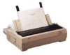
Primary, Secondary, Power Supply Circuit Block Diagram
 |
View all Epson FX 1170 manuals
Add to My Manuals
Save this manual to your list of manuals |
Page 64 highlights
REV.-A Primary Full Wave Rectification Circuit - Smoothing Circuit 9Filter Circuit AC input I I I I Secondary 1 I 1 1 I 1 Switching ; Smoothing < Circuit II1 Circuit 1 m I 1 1 I +5 v 1 1 Switching . 1 Regulator l------ 1 I 1 +5V 1 I Over Current I I I Control Circuit 1 I +5V 1 1 Over Voltage I 1 Control Circuit 1 t 1 I 1 ZD51 Photo- + coupler +35 V Line Detector Circuit . 4 + 3 5 VDC + +5 VDC I I { Photo- + coupler - 8A 1 1 1 1 I 1 1 1 1 1 I I t t I I I I I I I I 1 I I I I - 1 t 1 1 1 1 +5 V Line Voltage Overload Protection Circuit +35 V Line Voltage Drop Protection Circuit ZD53 - ~ Switch Figure 2-22. Power Supply Circuit Block Diagram 2-21
-
 1
1 -
2
-
3
-
4
-
5
-
6
-
7
-
8
-
9
-
10
-
11
-
12
-
13
-
14
-
15
-
16
-
17
-
18
-
19
-
20
-
21
-
22
-
23
-
24
-
25
-
26
-
27
-
28
-
29
-
30
-
31
-
32
-
33
-
34
-
35
-
36
-
37
-
38
-
39
-
40
-
41
-
42
-
43
-
44
-
45
-
46
-
47
-
48
-
49
-
50
-
51
-
52
-
53
-
54
-
55
-
56
-
57
-
58
-
 59
59 -
 60
60 -
 61
61 -
 62
62 -
 63
63 -
 64
64 -
 65
65 -
 66
66 -
 67
67 -
 68
68 -
 69
69 -
70
-
71
-
72
-
73
-
74
-
75
-
76
-
77
-
78
-
79
-
80
-
81
-
82
-
83
-
84
-
85
-
86
-
87
-
88
-
89
-
90
-
91
-
92
-
93
-
94
-
95
-
96
-
97
-
98
-
99
-
100
-
101
-
102
-
103
-
104
-
105
-
106
-
107
-
108
-
109
-
110
-
111
-
112
-
113
-
114
-
115
-
116
-
117
-
118
-
119
-
120
-
121
-
122
-
123
-
124
-
125
-
126
-
127
-
128
-
129
-
130
-
131
-
132
-
133
-
134
-
135
-
136
-
137
-
138
 |
 |

REV.-A
I
I
Primary
I
I
1
I
1
Secondary
1
I
1
Full Wave
Rectification
—
Smoothing
Switching
;
Smoothing
<
Circuit
Circuit
Circuit
I
Circuit
I
1
1
m
9
Filter Circuit
AC input
I
1
1
I
1
1
1
l------
1
I
1
1
I
I
I
I
1
I
1
1
I
1
1
t
1
+5
v
Switching
Regulator
. . . . . . . . . . . . . . .
.
+5V
Over Current
Control Circuit
----..-
.....
----
+5V
Over Voltage
Control Circuit
I
1
ZD51
Photo-
+35 V Line
coupler
+
Detector Circuit
I
8A
1
1
1
1
I
1
1
1
1
1
I
I
t
t
I
I
I
I
I
I
I
I
1
I
I
I
I
1
t
1
1
1
1
I
{
+5 V Line Voltage
ZD53
Photo-
+
Overload
coupler
Protection Circuit
-
—
.
—
+35 V Line
Voltage Drop
Protection Circuit
.
4
+35
VDC
+
+5
VDC
~
Switch
Figure 2-22. Power Supply Circuit Block Diagram
2-21