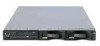
IBM 867431X Hardware Maintenance Manual - Page 52
System board, System board options connectors, System board jumper blocks
 |
View all IBM 867431X manuals
Add to My Manuals
Save this manual to your list of manuals |
Page 52 highlights
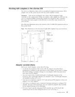
System board The illustrations in the following sections show the components on the system board. System board options connectors The following illustration identifies the connectors on the system board. C2T (in) port (U38) USB 1 port (J13) Management port (J53) Serial port A C2T (out) (J52) Serial port B port (U61) USB 2 port (J15) RS-485 (Advanced System Management interconnect) ports (J5) (J51) Ethernet ports (J1) BIOS code page jumper (J19) PCI slot 2 64 bit 33 MHz (J23) Remote Supervisor Adapter (J57) DIMM 4 (J47) DIMM 3 (J41) DIMM 2 (J34) DIMM 1 (J32) Microprocessor 2 (U79) Switch block (SW1) Battery PCI slot 1 64 bit 33 MHz (J10) Primary IDE (J7) Secondary IDE (J2) SCSI signal (J4) Power (J3) Power (J6) Diskette (J11) Microprocessor 1 (U47) Operator information panel (J43) Fan 5 (J35) Fan 3 (J22) Fan 6 (J38) Fan 4 (J24) SCSI hard disk drive power (J8) Fan 1 (J12) Fan 2 (J14) CD Power (J17) System board jumper blocks Any jumper blocks on the system board that are not shown in the illustration are reserved. For normal operation of the system, no jumpers should be installed on any of the jumper blocks. See "Recovering BIOS" on page 18 for information about the Flash ROM page-swap jumper. System board switch block The switch block contains microswitches 1-4. As pictured in this illustration, switch 1 is at the top of the switch block and switch 4 is at the bottom. For more information about this switch block see "Setting the password override switch" on page 31. 44 Hardware Maintenance Manual: xSeries 330 Type 8674, IntelliStation R Pro Type 6851, and Network Equipment Building System Type 8674
-
 1
1 -
2
-
3
-
4
-
5
-
6
-
7
-
8
-
9
-
10
-
11
-
12
-
13
-
14
-
15
-
16
-
17
-
18
-
19
-
20
-
21
-
22
-
23
-
24
-
25
-
26
-
27
-
28
-
29
-
30
-
31
-
32
-
33
-
34
-
35
-
36
-
37
-
38
-
39
-
40
-
41
-
42
-
43
-
44
-
45
-
46
-
 47
47 -
 48
48 -
 49
49 -
 50
50 -
 51
51 -
 52
52 -
 53
53 -
 54
54 -
 55
55 -
 56
56 -
 57
57 -
58
-
59
-
60
-
61
-
62
-
63
-
64
-
65
-
66
-
67
-
68
-
69
-
70
-
71
-
72
-
73
-
74
-
75
-
76
-
77
-
78
-
79
-
80
-
81
-
82
-
83
-
84
-
85
-
86
-
87
-
88
-
89
-
90
-
91
-
92
-
93
-
94
-
95
-
96
-
97
-
98
-
99
-
100
-
101
-
102
-
103
-
104
-
105
-
106
-
107
-
108
-
109
-
110
-
111
-
112
-
113
-
114
-
115
-
116
-
117
-
118
-
119
-
120
-
121
-
122
-
123
-
124
-
125
-
126
-
127
-
128
-
129
-
130
-
131
-
132
-
133
-
134
-
135
-
136
-
137
-
138
-
139
-
140
-
141
-
142
-
143
-
144
-
145
-
146
-
147
-
148
-
149
-
150
-
151
-
152
-
153
-
154
-
155
-
156
-
157
-
158
-
159
-
160
-
161
-
162
-
163
-
164
-
165
-
166
-
167
-
168
-
169
-
170
-
171
-
172
-
173
-
174
-
175
-
176
-
177
-
178
-
179
-
180
-
181
-
182
-
183
-
184
-
185
-
186
-
187
-
188
-
189
-
190
-
191
-
192
 |
 |
