Lenovo NetVista Hardware Maintenance Manual (HMM) for NetVista 6832 and 6833 s - Page 155
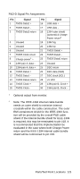
P&D-D Signal Pin Assignments, evaluated in the case where both Charge Power
 |
View all Lenovo NetVista manuals
Add to My Manuals
Save this manual to your list of manuals |
Page 155 highlights
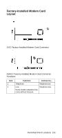
P&D-D Signal Pin Assignments Pin Signal 1 TMDS Data2 + 2 TMDS Data2 - 3 TMDS Data2 return 4 Unused 5 Unused 6 Unused 7 TMDS Clock return 8 Charge power1 + 9 1394 pair A, data 10 1394 pair A, data + 11 TMDS Data1 + 12 TMDS Data1 13 TMDS Data1 return 14 TMDS Clock + 15 TMDS Clock - Pin Signal 16 USB data + 17 USB data - 18 1394 outer shield (optional) & Charge Power return2 19 1394 Vg 20 1394 Vp 21 TMDS Data0 + 22 TMDS Data0 - 23 TMDS Data0 return 24 Unused 25 DDC return 26 DDC data (SDA) 27 DDC clock (SCL) 28 +5 VDC 29 1394 pair B, Clock + 30 1394 pair B, Clock - 1 Optional output from monitor. 2 Note: The IEEE-1394 internal cable bundle needs an outer shield to minimize internal crosstalk within the cable construction. The outer EMI containment shield for the IEEE-1394 function will be provided by the overall P&D cable shield. If the internal bundle shield for IEEE-1394 is required, this may be terminated to pin #18. It is recommended that this implementation be evaluated in the case where both Charge Power return and the IEEE-1394 internal cable bundle shield will be commoned to pin #18. Parts/Test Point Locations 123
-
 1
1 -
2
-
3
-
4
-
5
-
6
-
7
-
8
-
9
-
10
-
11
-
12
-
13
-
14
-
15
-
16
-
17
-
18
-
19
-
20
-
21
-
22
-
23
-
24
-
25
-
26
-
27
-
28
-
29
-
30
-
31
-
32
-
33
-
34
-
35
-
36
-
37
-
38
-
39
-
40
-
41
-
42
-
43
-
44
-
45
-
46
-
47
-
48
-
49
-
50
-
51
-
52
-
53
-
54
-
55
-
56
-
57
-
58
-
59
-
60
-
61
-
62
-
63
-
64
-
65
-
66
-
67
-
68
-
69
-
70
-
71
-
72
-
73
-
74
-
75
-
76
-
77
-
78
-
79
-
80
-
81
-
82
-
83
-
84
-
85
-
86
-
87
-
88
-
89
-
90
-
91
-
92
-
93
-
94
-
95
-
96
-
97
-
98
-
99
-
100
-
101
-
102
-
103
-
104
-
105
-
106
-
107
-
108
-
109
-
110
-
111
-
112
-
113
-
114
-
115
-
116
-
117
-
118
-
119
-
120
-
121
-
122
-
123
-
124
-
125
-
126
-
127
-
128
-
129
-
130
-
131
-
132
-
133
-
134
-
135
-
136
-
137
-
138
-
139
-
140
-
141
-
142
-
143
-
144
-
145
-
146
-
147
-
148
-
149
-
 150
150 -
 151
151 -
 152
152 -
 153
153 -
 154
154 -
 155
155 -
 156
156 -
 157
157 -
 158
158 -
 159
159 -
 160
160 -
161
-
162
-
163
-
164
-
165
-
166
-
167
-
168
-
169
-
170
-
171
-
172
-
173
-
174
-
175
-
176
-
177
-
178
-
179
-
180
-
181
-
182
-
183
-
184
-
185
-
186
-
187
-
188
-
189
-
190
-
191
-
192
-
193
-
194
-
195
-
196
-
197
-
198
-
199
-
200
-
201
-
202
-
203
-
204
-
205
-
206
-
207
-
208
-
209
-
210
-
211
 |
 |