Acer Aspire 6530G Aspire 6530/6530G Quick Guide - Page 145
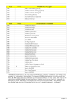
Chipset POST Codes, POST Code, Function, Phase, Component
 |
View all Acer Aspire 6530G manuals
Add to My Manuals
Save this manual to your list of manuals |
Page 145 highlights
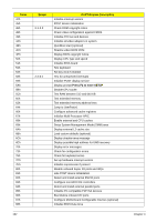
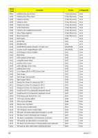
Chipset POST Codes The following table details the Chipset POST codes and components used in the POST. POST Code 0xA0 0x01 0x02 0x03 0x04 0x05 0x06 0x07 0x08 0x09 0x10 0x11 0x12 0x13 0x14 0x17 0x18 0x19 0x20 0x21 0x22 0x23 0x24 0x25 0x26 0x27 0x28 0x29 0x30 0x31 0x32 0x33 0x34 0x35 0x36 0x37 0x38 Function MRC Entry Enable MCHBAR Check ME existence Check for DRAM initialization interrupt and reset fail Determine the system Memory type based on first populated socket Verify all DIMMs are DDR2 and SO-DIMMS, which are unbuffered Verify all DIMMs are Non-ECC Verify all DIMMs are single or double sided and not mixed Verify all DIMMs are x8 or x16 width Calculate number of Row and Column bits Calculate number of banks for each DIMM Determine raw card type Find a common CAS latency between the DIMMS and the MCH Determine the memory frequency and CAS latency to program Determine the smallest common timing value for all DIMMS Power management resume Program DRAM type (DDR2/DDR3) and Power up sequence Program the correct system memory frequency Program the correct Graphics memory frequency Early DRC initialization Program the DRAM Row Attributes and DRAM Row Boundary registers PRE JEDEC. Program the RCOMP SRAM registers Program DRAM type (DDR2/DDR3) and Power up sequence Program the DRAM Timing Program the DRAM Bank Architecture register Enable all clocks on populated rows Program MCH ODT Program tRD Miscellaneous Pre JEDEC steps Program clock crossing registers Program the Egress port timings Program the Memory IO registers Perform steps required before JEDEC Perform JEDEC memory initialization for all memory rows Setup DRAM control register for normal operation and enable Do ZQ calibration for DDR3 Perform final Dra/Drb programming, Set the mode of operation for the memory channels Phase PEI PEI PEI PEI PEI PEI PEI PEI PEI PEI PEI PEI PEI PEI PEI PEI PEI PEI PEI PEI PEI PEI PEI PEI PEI PEI PEI PEI PEI PEI PEI PEI PEI PEI PEI PEI PEI Component chipset/MRC chipset/MRC chipset/MRC chipset/MRC chipset/MRC chipset/MRC chipset/MRC chipset/MRC chipset/MRC chipset/MRC chipset/MRC chipset/MRC chipset/MRC chipset/MRC chipset/MRC chipset/MRC chipset/MRC chipset/MRC chipset/MRC chipset/MRC chipset/MRC chipset/MRC chipset/MRC chipset/MRC chipset/MRC chipset/MRC chipset/MRC chipset/MRC chipset/MRC chipset/MRC chipset/MRC chipset/MRC chipset/MRC chipset/MRC chipset/MRC chipset/MRC chipset/MRC Chapter 4 135
-
 1
1 -
2
-
3
-
4
-
5
-
6
-
7
-
8
-
9
-
10
-
11
-
12
-
13
-
14
-
15
-
16
-
17
-
18
-
19
-
20
-
21
-
22
-
23
-
24
-
25
-
26
-
27
-
28
-
29
-
30
-
31
-
32
-
33
-
34
-
35
-
36
-
37
-
38
-
39
-
40
-
41
-
42
-
43
-
44
-
45
-
46
-
47
-
48
-
49
-
50
-
51
-
52
-
53
-
54
-
55
-
56
-
57
-
58
-
59
-
60
-
61
-
62
-
63
-
64
-
65
-
66
-
67
-
68
-
69
-
70
-
71
-
72
-
73
-
74
-
75
-
76
-
77
-
78
-
79
-
80
-
81
-
82
-
83
-
84
-
85
-
86
-
87
-
88
-
89
-
90
-
91
-
92
-
93
-
94
-
95
-
96
-
97
-
98
-
99
-
100
-
101
-
102
-
103
-
104
-
105
-
106
-
107
-
108
-
109
-
110
-
111
-
112
-
113
-
114
-
115
-
116
-
117
-
118
-
119
-
120
-
121
-
122
-
123
-
124
-
125
-
126
-
127
-
128
-
129
-
130
-
131
-
132
-
133
-
134
-
135
-
136
-
137
-
138
-
139
-
 140
140 -
 141
141 -
 142
142 -
 143
143 -
 144
144 -
 145
145 -
 146
146 -
 147
147 -
 148
148 -
 149
149 -
 150
150 -
151
-
152
-
153
-
154
-
155
-
156
-
157
-
158
-
159
-
160
-
161
-
162
-
163
-
164
-
165
-
166
-
167
-
168
-
169
-
170
-
171
-
172
-
173
-
174
-
175
-
176
-
177
-
178
-
179
-
180
-
181
-
182
-
183
-
184
-
185
-
186
-
187
-
188
-
189
-
190
-
191
-
192
-
193
-
194
-
195
-
196
-
197
-
198
-
199
-
200
-
201
-
202
-
203
-
204
-
205
-
206
-
207
-
208
-
209
-
210
-
211
-
212
-
213
-
214
-
215
-
216
-
217
-
218
-
219
-
220
-
221
-
222
-
223
-
224
 |
 |
