Hitachi HDS728080PLAT20 Specifications - Page 54
Addressing of registers
 |
UPC - 829686000094
View all Hitachi HDS728080PLAT20 manuals
Add to My Manuals
Save this manual to your list of manuals |
Page 54 highlights
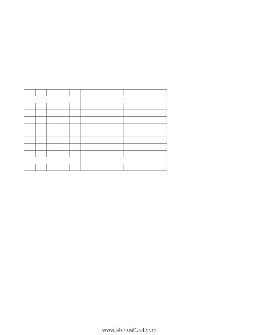
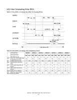
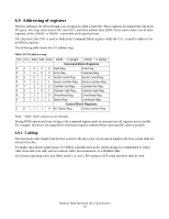
6.9 Addressing of registers The host addresses the drive through a set of registers called a Task File. These registers are mapped into the host's I/O space. Two chip select lines (CS0- and CS1-) and three address lines (DA0-2) are used to select one of these registers, while a DIOR- or DIOW- is provided at the specified time. The chip select line CS0- is used to address the Command Block registers while the CS1- is used to address Control Block registers. The following table shows the I/ O address map. Table 39: I/O address map CS0- CS1- DA2 DA1 DA0 DIOR- = 0 (Read) DIOW- = 0 (Write) Command Block Registers 01 0 0 0 Data Reg. Data Reg. 01 0 0 1 Error Reg. Features Reg. 01 0 1 0 Sector count Reg. Sector count Reg. 01 0 1 1 Sector number Reg. Sector number Reg. 01 1 0 0 Cylinder low Reg. Cylinder low Reg. 01 1 0 1 Cylinder high Reg. Cylinder high Reg. 01 1 1 0 Drive/Head Reg. Drive/Head Reg. 01 1 1 1 Status Reg. Command Reg. Control Block Registers 10 1 1 0 Alt. Status Reg. Device control Reg. Note: "Addr" field is shown as an example. During DMA operation (from writing to the command register until an interrupt) not all registers are accessible. For example, the host is not supposed to read status register contents before interrupt (the value is invalid). 6.9.1 Cabling The maximum cable length from the host system to the drive plus circuit pattern length in the host system shall not exceed 18 inches. For higher data transfer application (>8.3 MB/s) a modification in the system design is recommended to reduce cable noise and cross-talk, such as a shorter cable, bus termination, or a shielded cable. For systems operating with Ultra DMA mode 3, 4, and 5, 80-conductor ATA cable assembly shall be used. Deskstar 7K80 Hard Disk Drive Specification 50
-
 1
1 -
2
-
3
-
4
-
5
-
6
-
7
-
8
-
9
-
10
-
11
-
12
-
13
-
14
-
15
-
16
-
17
-
18
-
19
-
20
-
21
-
22
-
23
-
24
-
25
-
26
-
27
-
28
-
29
-
30
-
31
-
32
-
33
-
34
-
35
-
36
-
37
-
38
-
39
-
40
-
41
-
42
-
43
-
44
-
45
-
46
-
47
-
48
-
 49
49 -
 50
50 -
 51
51 -
 52
52 -
 53
53 -
 54
54 -
 55
55 -
 56
56 -
 57
57 -
 58
58 -
 59
59 -
60
-
61
-
62
-
63
-
64
-
65
-
66
-
67
-
68
-
69
-
70
-
71
-
72
-
73
-
74
-
75
-
76
-
77
-
78
-
79
-
80
-
81
-
82
-
83
-
84
-
85
-
86
-
87
-
88
-
89
-
90
-
91
-
92
-
93
-
94
-
95
-
96
-
97
-
98
-
99
-
100
-
101
-
102
-
103
-
104
-
105
-
106
-
107
-
108
-
109
-
110
-
111
-
112
-
113
-
114
-
115
-
116
-
117
-
118
-
119
-
120
-
121
-
122
-
123
-
124
-
125
-
126
-
127
-
128
-
129
-
130
-
131
-
132
-
133
-
134
-
135
-
136
-
137
-
138
-
139
-
140
-
141
-
142
-
143
-
144
-
145
-
146
-
147
-
148
-
149
-
150
-
151
-
152
-
153
-
154
-
155
-
156
-
157
-
158
-
159
-
160
-
161
-
162
-
163
-
164
-
165
-
166
-
167
-
168
-
169
-
170
-
171
-
172
-
173
-
174
-
175
-
176
-
177
-
178
-
179
-
180
-
181
-
182
-
183
-
184
-
185
-
186
-
187
-
188
-
189
-
190
-
191
-
192
-
193
-
194
-
195
-
196
-
197
-
198
-
199
-
200
-
201
-
202
-
203
-
204
-
205
-
206
-
207
-
208
-
209
-
210
-
211
-
212
-
213
-
214
-
215
-
216
-
217
-
218
-
219
-
220
-
221
-
222
-
223
-
224
-
225
-
226
-
227
-
228
-
229
-
230
-
231
-
232
-
233
-
234
-
235
-
236
-
237
-
238
-
239
-
240
-
241
-
242
-
243
-
244
-
245
-
246
-
247
-
248
-
249
-
250
-
251
-
252
-
253
-
254
-
255
-
256
-
257
-
258
 |
 |