AMD AMD-K6-2/450 Design Guide - Page 7
List of s - processor
 |
View all AMD AMD-K6-2/450 manuals
Add to My Manuals
Save this manual to your list of manuals |
Page 7 highlights
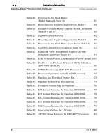
23913A/0-November 2000 Preliminary Information Embedded AMD-K6™ Processors BIOS Design Guide List of Figures Figure 1. CPUID Instruction Flow Chart 12 Figure 2. Extended Feature Enable Register (EFER) (Models 7 and 8/[7:0 18 Figure 3. Write Handling Control Register (WHCR) (Models 7 and 8/[7:0 20 Figure 4. SYSCALL/SYSRET Target Address Register (STAR) (Models 8, 9, and D 22 Figure 5. Extended Feature Enable Register (EFER) (Model 8/[F:8 24 Figure 6. Write Handling Control Register (WHCR) (Models 8/[F:8], 9, and D 28 Figure 7. UC/WC Cacheability Control Register (UWCCR) (Models 8/[F:8], 9, and D 31 Figure 8. Processor State Observability Register (PSOR) (Models 8/[F:8], 9, and Standard-Power D 34 Figure 9. Page Flush/Invalidate Register (PFIR) (Models 8/[F:8], 9, and D 36 Figure 10. Extended Feature Enable Register (EFER) (Models 9 and D 39 Figure 11. L2 Cache Organization (AMD-K6™-III Processor) . . . . . 40 Figure 12. L2 Cache Sector and Line Organization 41 Figure 13. L2 Tag or Data Location (AMD-K6™-III Processor)-EDX 41 Figure 14. L2 Data-EAX 42 Figure 15. L2 Tag Information (AMD-K6™-III Processor)-EAX . . 43 Figure 16. LRU Byte 43 Figure 17. Processor State Observability Register (PSOR) (Model D Low-Power Versions 46 Figure 18. L2 Cache Organization 48 Figure 19. L2 Cache Sector and Line Organization (same as Figure 12 49 List of Figures vii
-
 1
1 -
 2
2 -
 3
3 -
 4
4 -
 5
5 -
 6
6 -
 7
7 -
 8
8 -
 9
9 -
 10
10 -
 11
11 -
 12
12 -
13
-
14
-
15
-
16
-
17
-
18
-
19
-
20
-
21
-
22
-
23
-
24
-
25
-
26
-
27
-
28
-
29
-
30
-
31
-
32
-
33
-
34
-
35
-
36
-
37
-
38
-
39
-
40
-
41
-
42
-
43
-
44
-
45
-
46
-
47
-
48
-
49
-
50
-
51
-
52
-
53
-
54
-
55
-
56
-
57
-
58
-
59
-
60
-
61
-
62
-
63
-
64
-
65
-
66
-
67
-
68
-
69
-
70
-
71
-
72
-
73
-
74
-
75
-
76
-
77
-
78
-
79
-
80
-
81
-
82
-
83
-
84
-
85
-
86
-
87
-
88
-
89
-
90
-
91
-
92
-
93
-
94
-
95
-
96
-
97
-
98
 |
 |
