Epson TM U200D Technical Reference - Page 66

Printer Mechanism Drive Circuit - install

Page 66 highlights

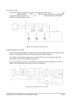
TM-U200D/U200PD Technical Manual Printer Mechanism Drive Circuit Print head drive circuit The head drive signal is output from CPU (U5) pin 64 to 72. Receiving this drive signal, the transistor array (QM1, QM2) and transistor array (QM3) turn On, Off, and drive the head. Power supply time to the head is adjusted by the supplied power voltage. CPU (U5) changes the power voltage between analog and digital at AN0 (pin 7) and decides and controls the head power supply time according to the internal time table. In order to prevent damage to the head during excessive printing, a heat Detector has been installed in the print head. An analog-digital conversion of the partial pressure difference between the heat Detector and R18 is carried out in AN1 (PIN8) of the CPU (U5) and the temperature is calculated. If the head is overheating or working improperly, the ERROR LED flashes. +24DT +5V U5 P60/ANO 7 V DTC P61/AN1 8 HD TEMP R46 D50 C29 R45 + _ C33 R8 R19 +5V R18 AVCC 5 AVSS 6 C31 C30 +5V C19 Q4 D27 D28 P47 71 P43 67 P42 66 P46 70 P44 68 P45 69 P41 65 72 P50 64 P40 HEAD1 Q5 HEAD5 HEAD6 Q7 HEAD2 Q12 HEAD4 HEAD3 Q9 HEAD7 HEAD9 Q11 HEAD8 Q6 D40 D44 Q8 D32 D38 RM3 7 8 5 6 3 4 D39 1 2 R20 Q13 Q10 D45 D41 D42 RM4 7 8 5 6 3 4 D43 1 2 QM1 1 8 9 6 7 4 5 2 3 1 0 QM2 1 8 9 6 7 4 5 2 3 1 D7 0 CN7 1 2 3 4 5 6 7 8 9 10 11 12 13 14 15 Printwhbehadj ub ng it FG # 2 # 4 # 6 # 8 COM (# 4.6.8 ) # 9 C0M ( # 1.2.9 ) THEM1 THEM2 COM (# 3.5.7 ) # 5 # 7 # 1 # 3 +24A Figure 2-24 Print head drive circuit Rev. B Mechanism Configuration and Operating Principles

  • 1
  • 2
  • 3
  • 4
  • 5
  • 6
  • 7
  • 8
  • 9
  • 10
  • 11
  • 12
  • 13
  • 14
  • 15
  • 16
  • 17
  • 18
  • 19
  • 20
  • 21
  • 22
  • 23
  • 24
  • 25
  • 26
  • 27
  • 28
  • 29
  • 30
  • 31
  • 32
  • 33
  • 34
  • 35
  • 36
  • 37
  • 38
  • 39
  • 40
  • 41
  • 42
  • 43
  • 44
  • 45
  • 46
  • 47
  • 48
  • 49
  • 50
  • 51
  • 52
  • 53
  • 54
  • 55
  • 56
  • 57
  • 58
  • 59
  • 60
  • 61
  • 62
  • 63
  • 64
  • 65
  • 66
  • 67
  • 68
  • 69
  • 70
  • 71
  • 72
  • 73
  • 74
  • 75
  • 76
  • 77
  • 78
  • 79
  • 80
  • 81
  • 82
  • 83
  • 84
  • 85
  • 86
  • 87
  • 88
  • 89
  • 90
  • 91
  • 92
  • 93
  • 94
  • 95
  • 96
  • 97
  • 98
  • 99
  • 100
  • 101
  • 102
  • 103
  • 104
  • 105
  • 106
  • 107
  • 108
  • 109
  • 110
  • 111
  • 112
  • 113
  • 114
  • 115
  • 116
  • 117
  • 118
  • 119
  • 120
  • 121
  • 122
  • 123
  • 124
  • 125
  • 126
  • 127
  • 128
  • 129
  • 130
  • 131
  • 132
  • 133
  • 134
  • 135
  • 136
  • 137
  • 138
  • 139
  • 140
  • 141
  • 142
  • 143
  • 144
  • 145
  • 146
  • 147
  • 148
  • 149
  • 150
  • 151
  • 152
  • 153
  • 154
  • 155
  • 156
  • 157
  • 158
  • 159
  • 160
  • 161
  • 162
  • 163
  • 164
  • 165
  • 166
  • 167
  • 168
  • 169

Rev. B
Mechanism Configuration and Operating Principles
TM-U200D/U200PD Technical Manual
Printer Mechanism Drive Circuit
Print head drive circuit
The head drive signal is output from CPU (U5) pin 64 to 72. Receiving this drive signal, the
transistor array (QM1, QM2) and transistor array (QM3) turn On, Off, and drive the head.
Power supply time to the head is adjusted by the supplied power voltage. CPU (U5) changes the
power voltage between analog and digital at AN0 (pin 7) and decides and controls the head
power supply time according to the internal time table.
In order to prevent damage to the head during excessive printing, a heat Detector
has been
installed in the print head. An analog-digital conversion of the partial pressure difference
between the heat Detector
and R18 is carried out in AN1 (PIN8) of the CPU (U5) and the
temperature is calculated. If the head is overheating or working improperly, the ERROR LED
flashes.
Figure 2-24
Print head drive circuit
COM (# 3.5.7 )
# 5
# 7
# 1
# 3
wbh
jbg
HEAD1
HEAD5
HEAD6
HEAD2
RM3
8
7
6
5
4
3
2
1
Q4
9
7
5
3
8
6
4
2
1
1
0
QM1
Q6
Q5
Q7
+5V
RM4
8
7
6
5
4
3
2
1
Q8
9
7
5
3
8
6
4
2
1
1
0
QM2
Q10
Q9
Q11
HEAD3
HEAD7
HEAD9
HEAD8
+24A
D7
68
69
65
72
Q12
R20
1
2
3
CN7
4
5
6
7
8
9
10
11
12
13
14
15
P44
P45
P41
P50
HEAD4
67
66
70
P43
P42
P46
71
P47
64
P40
8
HD
TEMP
P61/AN1
7
V
DTC
P60/ANO
6
AVSS
5
AVCC
C30
C31
R45
R46
R18
C19
C29
R8
+
C33
_
R19
+24DT
# 9
C0M ( # 1.2.9 )
THEM1
THEM2
# 4
# 6
# 8
COM (# 4.6.8 )
# 2
FG
D27
D28
Q13
U5
+5V
+5V
D50
D32
D38
D39
D40
D41
D42
D43
D45
D44